概要信息:
TLC5618C, TLC5618I
PROGRAMMABLE DUAL 12-BIT DIGITAL-TO-ANALOG CONVERTERS
SLAS156 – JULY 1997
1POST OFFICE BOX 655303 • DALLAS, TEXAS 75265
� Programmable Settling Time to 0.5 LSB
3 µs or 15 µs Typ
� Two 12-Bit CMOS Voltage Output DACs in
an 8-Pin Package
� Simultaneous Updates for DAC A
and DAC B
� Single Supply Operation
� 3 Wire Serial Interface
� High-Impedance Reference Inputs
� Voltage Output Range . . . 2 Times the
Reference Input Voltage
� Software Power Down Mode
� Internal Power-On Reset
� Low Power Consumption:
3 mW Typ in Slow Mode
8 mW Typ in Fast Mode
� Input Data Update Rate of 1.21 MHz
� Monotonic Over Temperature
applications
� Battery Powered Test Instruments
� Digital Offset and Gain Adjustment
� Battery Operated/Remote Industrial
Controls
� Machine and Motion Control Devices
� Cellular Telephones
description
The TLC5618 is a dual 12-bit voltage output
digital-to-analog converter (DAC) with buffered
reference inputs (high impedance). The DACs
have an output voltage range that is two times the
reference voltage, and the DACs are monotonic.
The device is simple to use, running from a single
supply of 5 V. A power-on reset function is
incorporated to ensure repeatable start-up
conditions.
Digital control of the TLC5618 is over a 3-wire CMOS-compatible serial bus. The device receives a 16-bit word
for programming and to produce the analog output. The digital inputs feature Schmitt triggers for high noise
immunity. Digital communication protocols include the SPI , QSPI , and Microwire standards.
The 8-terminal small-outline D package allows digital control of analog functions in space-critical applications.
The TLC5618C is characterized for operation from 0°C to 70°C. The TLC5618I is characterized for operation
from –40°C to 85°C.
AVAILABLE OPTIONS
PACKAGE
TA
SMALL OUTLINE†
(D)
PLASTIC DIP
(P)
0°C to 70°C TLC5618CD TLC5618CP
–40°C to 85°C TLC5618ID TLC5618IP
† Available in tape and reel as the TLC5618CDR and the TLC5618IDR
Please be aware that an important notice concerning availability, standard warranty, and use in critical applications of
Texas Instruments semiconductor products and disclaimers thereto appears at the end of this data sheet.
SPI and QSPI are trademarks of Motorola, Inc.
Microwire is a trademark of National Semiconductor Corporation.
Copyright 1997, Texas Instruments IncorporatedPRODUCTION DATA information is current as of publication date.
Products conform to specifications per the terms of Texas Instruments
standard warranty. Production processing does not necessarily include
testing of all parameters.
1
2
3
4
8
7
6
5
DIN
SCLK
CS
OUT A
VDD
OUT B
REFIN
AGND
D OR P PACKAGE
(TOP VIEW)
TLC5618C, TLC5618I
PROGRAMMABLE DUAL 12-BIT DIGITAL-TO-ANALOG CONVERTERS
SLAS156 – JULY 1997
2 POST OFFICE BOX 655303 • DALLAS, TEXAS 75265
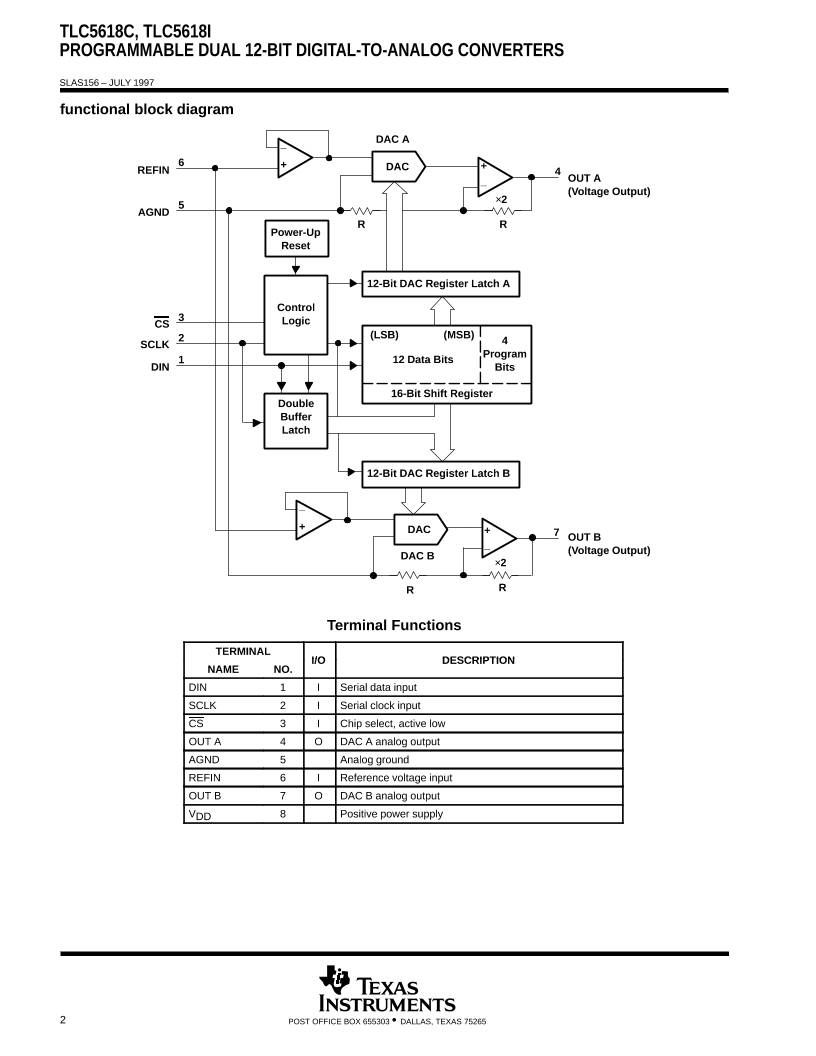
functional block diagram
_
+DAC
12-Bit DAC Register Latch A
Power-Up
Reset
Control
Logic
16-Bit Shift Register
4
Program
Bits
12 Data Bits
(LSB) (MSB)
REFIN
AGND
CS
SCLK
DIN
OUT A
(Voltage Output)
_
+
R R
DAC A
×2
Double
Buffer
Latch
_
+
_
+
OUT B
(Voltage Output)DAC B
DAC
R
×2
R
12-Bit DAC Register Latch B
7
4
6
5
3
2
1
Terminal Functions
TERMINAL
I/O DESCRIPTION
NAME NO.
DIN 1 I Serial data input
SCLK 2 I Serial clock input
CS 3 I Chip select, active low
OUT A 4 O DAC A analog output
AGND 5 Analog ground
REFIN 6 I Reference voltage input
OUT B 7 O DAC B analog output
VDD 8 Positive power supply
TLC5618C, TLC5618I
PROGRAMMABLE DUAL 12-BIT DIGITAL-TO-ANALOG CONVERTERS
SLAS156 – JULY 1997
3POST OFFICE BOX 655303 • DALLAS, TEXAS 75265
absolute maximum ratings over operating free-air temperature range (unless otherwise noted)†
Supply voltage (VDD to AGND) 7 V. . . . . . . . . . . . . . . . . . . . . . . . . . . . . . . . . . . . . . . . . . . . . . . . . . . . . . . . . . . . . . .
Digital input voltage range to AGND – 0.3 V to VDD + 0.3 V. . . . . . . . . . . . . . . . . . . . . . . . . . . . . . . . . . . . . . . . . .
Reference input voltage range to AGND – 0.3 V to VDD + 0.3 V. . . . . . . . . . . . . . . . . . . . . . . . . . . . . . . . . . . . . .
Output voltage at OUT from external source VDD + 0.3 V. . . . . . . . . . . . . . . . . . . . . . . . . . . . . . . . . . . . . . . . . . . .
Continuous current at any terminal ±20 mA. . . . . . . . . . . . . . . . . . . . . . . . . . . . . . . . . . . . . . . . . . . . . . . . . . . . . . . .
Operating free-air temperature range, TA: TLC5618C 0°C to 70°C. . . . . . . . . . . . . . . . . . . . . . . . . . . . . . . . . . . .
TLC5618I –40°C to 85°C. . . . . . . . . . . . . . . . . . . . . . . . . . . . . . . . . . .
Storage temperature range, Tstg –65°C to 150°C. . . . . . . . . . . . . . . . . . . . . . . . . . . . . . . . . . . . . . . . . . . . . . . . . . .
Lead temperature 1,6 mm (1/16 inch) from case for 10 seconds 260°C. . . . . . . . . . . . . . . . . . . . . . . . . . . . . . .
† Stresses beyond those listed under “absolute maximum ratings” may cause permanent damage to the device. These are stress ratings only, and
functional operation of the device at these or any other conditions beyond those indicated under “recommended operating conditions” is not
implied. Exposure to absolute-maximum-rated conditions for extended periods may affect device reliability.
recommended operating conditions
MIN NOM MAX UNIT
Supply voltage, VDD 4.5 5 5.5 V
High-level digital input voltage, VIH VDD = 5 V 0.7 VDD V
Low-level digital input voltage, VIL VDD = 5 V 0.3 VDD V
Reference voltage, Vref to REFIN terminal 2 2.048 VDD–1.1 V
Load resistance, RL 2 kΩ
Operating free-air temperature TA
TLC5618C 0 70 °C
,
TLC5618I –40 85 °C
TLC5618C, TLC5618I
PROGRAMMABLE DUAL 12-BIT DIGITAL-TO-ANALOG CONVERTERS
SLAS156 – JULY 1997
4 POST OFFICE BOX 655303 • DALLAS, TEXAS 75265
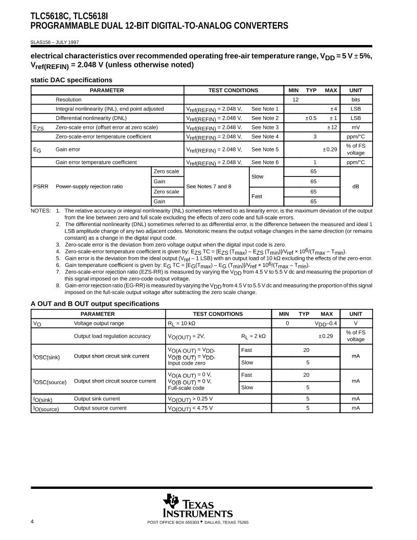
electrical characteristics over recommended operating free-air temperature range, VDD = 5 V ± 5%,
Vref(REFIN) = 2.048 V (unless otherwise noted)
static DAC specifications
PARAMETER TEST CONDITIONS MIN TYP MAX UNIT
Resolution 12 bits
Integral nonlinearity (INL), end point adjusted Vref(REFIN) = 2.048 V, See Note 1 ±4 LSB
Differential nonlinearity (DNL) Vref(REFIN) = 2.048 V, See Note 2 ±0.5 ± 1 LSB
EZS Zero-scale error (offset error at zero scale) Vref(REFIN) = 2.048 V, See Note 3 ±12 mV
Zero-scale-error temperature coefficient Vref(REFIN) = 2.048 V, See Note 4 3 ppm/°C
EG Gain error Vref(REFIN) = 2.048 V, See Note 5 ±0.29
% of FS
voltage
Gain error temperature coefficient Vref(REFIN) = 2.048 V, See Note 6 1 ppm/°C
PSRR P l j i i
Zero scale
S N 7 d 8
Slow
65
dBower-supp y re ect on rat o
Gain
ee otes an
65
Zero scale
Fast
65
Gain 65
NOTES: 1. The relative accuracy or integral nonlinearity (INL) sometimes referred to as linearity error, is the maximum deviation of the output
from the line between zero and full scale excluding the effects of zero code and full-scale errors.
2. The differential nonlinearity (DNL) sometimes referred to as differential error, is the difference between the measured and ideal 1
LSB amplitude change of any two adjacent codes. Monotonic means the output voltage changes in the same direction (or remains
constant) as a change in the digital input code.
3. Zero-scale error is the deviation from zero voltage output when the digital input code is zero.
4. Zero-scale-error temperature coefficient is given by: EZS TC = [EZS (Tmax) – EZS (Tmin)]/Vref × 106/(Tmax – Tmin).
5. Gain error is the deviation from the ideal output (Vref – 1 LSB) with an output load of 10 kΩ excluding the effects of the zero-error.
6. Gain temperature coefficient is given by: EG TC = [EG(Tmax) – EG (Tmin)]/Vref × 106/(Tmax – Tmin).
7. Zero-scale-error rejection ratio (EZS-RR) is measured by varying the VDD from 4.5 V to 5.5 V dc and measuring the proportion of
this signal imposed on the zero-code output voltage.
8. Gain-error rejection ratio (EG-RR) is measured by varying the VDD from 4.5 V to 5.5 V dc and measuring the proportion of this signal
imposed on the full-scale output voltage after subtracting the zero scale change.
A OUT and B OUT output specifications
PARAMETER TEST CONDITIONS MIN TYP MAX UNIT
VO Voltage output range RL = 10 kΩ 0 VDD–0.4 V
Output load regulation accuracy VO(OUT) = 2V, RL = 2 kΩ ±0.29
% of FS
voltage
IOSC(sink) Output short circuit sink current
VO(A OUT) = VDD,
VO(B OUT) = VDD
Fast 20
mA ,
Input code zero Slow 5
IOSC(source) Output short circuit source current
VO(A OUT) = 0 V,
VO(B OUT) = 0 V
Fast 20
mA ,
Full-scale code Slow 5
IO(sink) Output sink current VO(OUT) > 0.25 V 5 mA
IO(source) Output source current VO(OUT) < 4.75 V 5 mA
TLC5618C, TLC5618I
PROGRAMMABLE DUAL 12-BIT DIGITAL-TO-ANALOG CONVERTERS
SLAS156 – JULY 1997
5POST OFFICE BOX 655303 • DALLAS, TEXAS 75265
electrical characteristics over recommended operating free-air temperature range, VDD = 5 V ± 5%,
Vref(REFIN) = 2.048 V (unless otherwise noted) (continued)
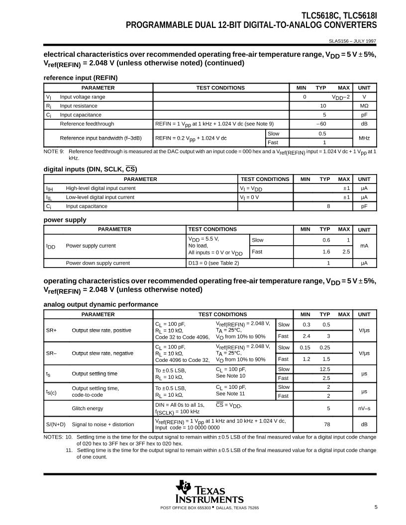
reference input (REFIN)
PARAMETER TEST CONDITIONS MIN TYP MAX UNIT
VI Input voltage range 0 VDD–2 V
Ri Input resistance 10 MΩ
Ci Input capacitance 5 pF
Reference feedthrough REFIN = 1 Vpp at 1 kHz + 1.024 V dc (see Note 9) –60 dB
Reference input bandwidth (f–3dB) REFIN = 0 2 Vpp + 1 024 V dc
Slow 0.5
MHz . .
Fast 1
NOTE 9: Reference feedthrough is measured at the DAC output with an input code = 000 hex and a Vref(REFIN) input = 1.024 V dc + 1 Vpp at 1
kHz.
digital inputs (DIN, SCLK, CS)
PARAMETER TEST CONDITIONS MIN TYP MAX UNIT
IIH High-level digital input current VI = VDD ±1 µA
IIL Low-level digital input current VI = 0 V ±1 µA
Ci Input capacitance 8 pF
power supply
PARAMETER TEST CONDITIONS MIN TYP MAX UNIT
IDD Power supply current
VDD = 5.5 V,
No load
Slow 0.6 1
mA ,
All inputs = 0 V or VDD Fast 1.6 2.5
Power down supply current D13 = 0 (see Table 2) 1 µA
operating characteristics over recommended operating free-air temperature range, VDD = 5 V ± 5%,
Vref(REFIN) = 2.048 V (unless otherwise noted)
analog output dynamic performance
PARAMETER TEST CONDITIONS MIN TYP MAX UNIT
SR+ Output slew rate positive
CL = 100 pF,
RL = 10 kΩ
Vref(REFIN) = 2.048 V,
TA = 25°C
Slow 0.3 0.5
V/µs , ,
Code 32 to Code 4096,
,
VO from 10% to 90% Fast 2.4 3
SR– Output slew rate negative
CL = 100 pF,
RL = 10 kΩ
Vref(REFIN) = 2.048 V,
TA = 25°C
Slow 0.15 0.25
V/µs , ,
Code 4096 to Code 32,
,
VO from 10% to 90% Fast 1.2 1.5
ts Output settling time
To ±0.5 LSB, CL = 100 pF,
S N 10
Slow 12.5
µs
RL = 10 kΩ, ee ote Fast 2.5
ts(c)
Output settling time, To ±0.5 LSB, CL = 100 pF,
S N 11
Slow 2
µs
code-to-code RL = 10 kΩ, ee ote Fast 2
Glitch energy
DIN = All 0s to all 1s,
f(SCLK) = 100 kHz
CS = VDD,
5 nV–s
S/(N+D) Signal to noise + distortion
Vref(REFIN) = 1 Vpp at 1 kHz and 10 kHz + 1.024 V dc,
Input code = 10 0000 0000
78 dB
NOTES: 10. Settling time is the time for the output signal to remain within ±0.5 LSB of the final measured value for a digital input code change
of 020 hex to 3FF hex or 3FF hex to 020 hex.
11. Settling time is the time for the output signal to remain within ±0.5 LSB of the final measured value for a digital input code change
of one count.
TLC5618C, TLC5618I
PROGRAMMABLE DUAL 12-BIT DIGITAL-TO-ANALOG CONVERTERS
SLAS156 – JULY 1997
6 POST OFFICE BOX 655303 • DALLAS, TEXAS 75265
operating characteristics over recommended operating free-air temperature range, VDD = 5 V ± 5%,
Vref(REFIN) = 2.048 V (unless otherwise noted) (continued)
digital input timing requirements
MIN NOM MAX UNIT
tsu(DS) Setup time, DIN before SCLK low 5 ns
th(DH) Hold time, DIN valid after SCLK low 5 ns
tsu(CSS) Setup time, CS low to SCLK low 5 ns
tsu(CS1) Setup time, CS high to SCLK low 5 ns
tw(CL) Pulse duration, SCLK low 25 ns
tw(CH) Pulse duration, SCLK high 25 ns
ÎÎÎÎÎ
ÎÎÎÎÎ
ÎÎÎÎÎ
ÎÎÎÎÎÎÎ
ÎÎÎÎÎÎÎ
ÎÎÎÎÎÎÎ
tsu(CSS)
tw(CL) tw(CH) tsu(CS1)
CS
SCLK
DIN
tsu(DS) th(DH)
D15 D14 D13 D12 D11 D0
ÏÏ ts
DAC A/B
OUT
(see Note A) (see Note A)
NOTE A: The input clock, applied at the SCLK terminal, should be inhibited low when CS is high to minimize clock feedthrough.
ÏÏÏÏÏÏProgram Bits (4)
ÏÏÏÏ
ÏÏÏÏ
DAC Data
Bits (12)
≤ Final Value ± 0.5 LSB
Figure 1. Timing Diagram
TLC5618C, TLC5618I
PROGRAMMABLE DUAL 12-BIT DIGITAL-TO-ANALOG CONVERTERS
SLAS156 – JULY 1997
7POST OFFICE BOX 655303 • DALLAS, TEXAS 75265
TYPICAL CHARACTERISTICS
Figure 2
15
10
0
–5
0 1 2
O
u
tp
u
t
S
in
k
C
u
rr
en
t
–
m
A
20
25
Output Load Voltage – V
OUTPUT SINK CURRENT (FAST MODE)
vs
OUTPUT LOAD VOLTAGE
30
3.5
5
35
40
1.50.5 2.5 3 4 4.5
VCC = 5 V
Input Code = 0
Figure 3
–30
–20
–10
0
O
u
tp
u
t
S
o
u
rc
e
C
u
rr
en
t
–
m
A
–40
–50
Output Load Voltage – V
OUTPUT SOURCE CURRENT (FAST MODE)
vs
OUTPUT LOAD VOLTAGE
–60
0 0.5 1 1.5 2 2.5 3 3.5 4 4.5
VDD = 5 V
Input Code = 4095
Figure 4
10
5
0
–0
O
u
tp
u
t
S
in
k
C
u
rr
en
t
–
m
A
15
20
Output Load Voltage – V
OUTPUT SINK CURRENT (SLOW MODE)
vs
OUTPUT LOAD VOLTAGE
25
0 0.5 1 1.5 2 2.5 3 3.5 4 4.5
VDD = 5 V
Input Code = 0
Figure 5
–15
–10
–5
0
O
u
tp
u
t
S
o
u
rc
e
C
u
rr
en
t
–
m
A
–20
–25
Output Load Voltage – V
OUTPUT SOURCE CURRENT (SLOW MODE)
vs
OUTPUT LOAD VOLTAGE
–30
0 0.5 1 1.5 2 2.5 3 3.5 4 4.5
VDD = 5 V
Input Code = 4095
TLC5618C, TLC5618I
PROGRAMMABLE DUAL 12-BIT DIGITAL-TO-ANALOG CONVERTERS
SLAS156 – JULY 1997
8 POST OFFICE BOX 655303 • DALLAS, TEXAS 75265
TYPICAL CHARACTERISTICS
Figure 6
0.4S
u
p
p
ly
C
u
rr
en
t
–
m
A 1
1.4
SUPPLY CURRENT
vs
TEMPERATURE
1.2
0.8
0.6
0.2
0
–60 –40 –20 0 20 40 60 80 100 120 140
Temperature – °C
VDD = 5 V
VREFIN = 2.048 V
TA = 25°C
Fast Mode
Slow Mode
Figure 7
–10
–15
–20
–30
100 1000
R
el
at
iv
e
G
ai
n
–
d
B
–5
0
f – Frequency – kHz
RELATIVE GAIN (FAST MODE)
vs
FREQUENCY
5
10 K
–25
VCC = 5 V
VREFIN = 0.2 VPP + 2.048 Vdc
TA = 25°C
Figure 8
–10
–15
–20
–30
100 1000
R
el
at
iv
e
G
ai
n
–
d
B
–5
0
f – Frequency – kHz
RELATIVE GAIN (SLOW MODE)
vs
FREQUENCY
5
10 K
–25
VCC = 5 V
VREFIN = 0.2 VPP +
2.048 Vdc
TA = 25°C
–35
–40
Figure 9
80
75
70
65
1 10
T
H
D
–
T
o
ta
l H
ar
m
o
n
ic
D
is
to
rt
io
n
–
d
B
85
90
f – Frequency – kHz
TOTAL HARMONIC DISTORTION (SLOW MODE)
vs
FREQUENCY
95
100
TLC5618C, TLC5618I
PROGRAMMABLE DUAL 12-BIT DIGITAL-TO-ANALOG CONVERTERS
SLAS156 – JULY 1997
9POST OFFICE BOX 655303 • DALLAS, TEXAS 75265
TYPICAL CHARACTERISTICS
Figure 10
70
65
60
1 10
T
H
D
+N
–
T
o
ta
l H
ar
m
o
n
ic
D
is
to
rt
io
n
+
N
o
is
e
–
d
B
75
80
f – Frequency– kHz
TOTAL HARMONIC DISTORTION + NOISE (SLOW MODE)
vs
FREQUENCY
85
100
Figure 11
75
70
65
1 10
S
N
R
–
S
ig
n
al
-T
o
-N
o
is
e
R
at
io
–
d
B
80
f – Frequency– kHz
SIGNAL-TO-NOISE RATIO (SLOW MODE)
vs
FREQUENCY
85
100
Figure 12
85
80
75
1 10
T
H
D
–
T
o
ta
l H
ar
m
o
n
ic
D
is
to
rt
io
n
–
d
B
90
f – Frequency – kHz
TOTAL HARMONIC DISTORTION (FAST MODE)
vs
FREQUENCY
95
100
Figure 13
75
70
65
1 10
T
H
D
+N
–
T
o
ta
l H
ar
m
o
n
ic
D
is
to
rt
io
n
+
N
o
is
e
–
d
B
80
f – Frequency – kHz
TOTAL HARMONIC DISTORTION + NOISE (FAST MODE)
vs
FREQUENCY
85
100
TLC5618C, TLC5618I
PROGRAMMABLE DUAL 12-BIT DIGITAL-TO-ANALOG CONVERTERS
SLAS156 – JULY 1997
10 POST OFFICE BOX 655303 • DALLAS, TEXAS 75265
TYPICAL CHARACTERISTICS
75
70
65
1 10
S
N
R
–
S
ig
n
al
-T
o
-N
o
is
e
R
at
io
–
d
B
80
f – Frequency – kHz
SIGNAL-TO-NOISE RATIO (FAST MODE)
vs
FREQUENCY
85
100
Figure 14
TLC5618C, TLC5618I
PROGRAMMABLE DUAL 12-BIT DIGITAL-TO-ANALOG CONVERTERS
SLAS156 – JULY 1997
11POST OFFICE BOX 655303 • DALLAS, TEXAS 75265
TYPICAL CHARACTERISTICS
D
N
L
–
D
if
fe
re
n
ti
al
N
o
n
lin
ea
ri
ty
–
L
S
B
–0.4
0.4
0.2
0
–0.1
0.3
0.1
–0.2
–0.3
Input Code
1023 2047 3071 40950
Figure 15. Differential Nonlinearity With Input Code
IN
L
–
In
te
g
ra
l N
o
n
lin
ea
ri
ty
–
L
S
B
–3
Input Code
5
0
–1
1023 2047 3071 40950
4
3
2
1
–2
–4
–5
Figure 16. Integral Nonlinearity With Input Code
TLC5618C, TLC5618I
PROGRAMMABLE DUAL 12-BIT DIGITAL-TO-ANALOG CONVERTERS
SLAS156 – JULY 1997
12 POST OFFICE BOX 655303 • DALLAS, TEXAS 75265
APPLICATION INFORMATION
general function
The TLC5618 uses a resistor string network buffered with an op amp to convert 12-bit digital data to analog
voltage levels (see functional block diagram and Figure 17). The output is the same polarity as the reference
input (see Table 1).
The output code is given by: 2�VREFIN
�CODE
4096
An internal circuit resets the DAC register to all 0s on power-up.
_
+
Resistor
String
DAC
5 V
0.1 µF
AGND VDD
OUT
REFIN
R
R
_
+
×2DIN
CS
SCLK
Figure 17. TLC5618 Typical Circuit
Table 1. Binary Code Table (0 V to 2 VREFIN Output), Gain = 2
INPUT OUTPUT
1111 1111 1111 2�VREFIN
� 4095
4096
: :
1000 0000 0001 2�VREFIN
�2049
4096
1000 0000 0000 2�VREFIN
� 2048
4096
� VREFIN
0111 1111 1111 2�VREFIN
� 2047
4096
: :
0000 0000 0001 2�VREFIN
� 1
4096
0000 0000 0000 0 V
TLC5618C, TLC5618I
PROGRAMMABLE DUAL 12-BIT DIGITAL-TO-ANALOG CONVERTERS
SLAS156 – JULY 1997
13POST OFFICE BOX 655303 • DALLAS, TEXAS 75265
APPLICATION INFORMATION
buffer amplifier
The output buffer has a rail-to-rail output with short circuit protection and can drive a 2-kΩ load with a 100 pF
load capacitance. Settling time is a software selectable 15 µs or 3 µs, typical to within ± 0.5 LSB of final value.
external reference
The reference voltage input is buffered which makes the DAC input resistance not code dependent. Therefore,
the REFIN input resistance is 10 MΩ and the REFIN input capacitance is typically 5 pF, independent of input
code. The reference voltage determines the DAC full-scale output.
logic interface
The logic inputs function with CMOS logic levels. Most of the standard high-speed CMOS logic families may
be used.
serial clock and update rate
Figure 1 shows the TLC5618 timing. The maximum serial clock rate is
f(SCLK)max � 1
tw�CH�min� tw�CL�min
� 20 MHz
The digital update rate is limited by the chip-select period, which is
tp(CS) � 16��tw�CH� � tw�CL�
�� tsu�CS1�
This equals an 820-ns or 1.21-MHz update rate. However, the DAC settling time to 12 bits limits the update rate
for full-scale input step transitions.
serial interface
When chip select (CS) is low, the input data is read into a 16-bit shift register with the input data clocked in most
significant bit first. The falling edge of the SCLK input shifts the data into the input register.
The rising edge of CS then transfers the data to the DAC register. When CS is high, input data cannot be clocked
into the input register. All CS transitions should occur when the SCLK input is low.
The 16 bits of data can be transferred with the sequence shown in Figure 18.
D15 D14 D13 D12 D11 12 Data Bits D0
Program Bits Data Bits
16 Bits
MSB (Input Word) MSB (Data) LSB (Data, Input Word)
Figure 18. Input Data Word Format
TLC5618C, TLC5618I
PROGRAMMABLE DUAL 12-BIT DIGITAL-TO-ANALOG CONVERTERS
SLAS156 – JULY 1997
14 POST OFFICE BOX 655303 • DALLAS, TEXAS 75265
APPLICATION INFORMATION
Table 2 shows the function of program bits D15 – D12.
Table 2. Program Bits D15 – D12 Function
PROGRAM BITS
DEVICE FUNCTION
D15 D14 D13 D12
1 X X X
Write to latch A with serial
interface register data and latch B
updated with buffer latch data
0 X X 0
Write to latch B and double buffer
latch
0 X X 1 Write to double buffer latch only
X 1 X X 12.5 µs settling time
X 0 X X 2.5 µs settling time
X X 0 X Powered-up operation
X X 1 X Power down mode
function of the latch control bits (D15 and D12)
Three data transfers are possible. All transfers occur immediately after CS goes high and are described in the
following sections.
latch A write, latch B update (D15 = high, D12 = X)
The serial interface register (SIR) data are written to latch A and the double buffer latch contents are written to
latch B. The double buffer contents are unaffected. This program bit condition allows simultaneous output
updates of both DACs.
Serial
Interface
Register
D12 = X
D15 = High
Latch A
Latch B
Double
Buffer Latch
To DAC A
To DAC B
Figure 19. Latch A Write, Latch B Update
latch B and double-buffer 1 write (D15 = low, D12 = low)
The SIR data are written to both latch B and the double buffer. Latch A is unaffected.
Serial
Interface
Register
D12 = Low
D15 = Low
Latch A
Latch B
Double
Buffer Latch
To DAC A
To DAC B
Figure 20. Latch B and Double-Buffer Write
TLC5618C, TLC5618I
PROGRAMMABLE DUAL 12-BIT DIGITAL-TO-ANALOG CONVERTERS
SLAS156 – JULY 1997
15POST OFFICE BOX 655303 • DALLAS, TEXAS 75265
APPLICATION INFORMATION
double-buffer-only write (D15 = low, D12 = high)
The SIR data are written to the double buffer only. Latch A and B contents are unaffected.
Serial
Interface
Register
D12 = High
D15 = Low
Latch A
Latch B
Double
Buffer
To DAC A
To DAC B
Figure 21. Double-Buffer-Only Write
purpose and use of the double buffer
Normally only one DAC output can change after a write. The double buffer allows both DAC outputs to change
after a single write. This is achieved by the two following steps.
1. A double-buffer-only write is executed to store the new DAC B data without changing the DAC A and B
outputs.
2. Following the previous step, a write to latch A is executed. This writes the SIR data to latch A and also
writes the double-buffer contents to latch B. Thus both DACs receive their new data at the same time
and so both DAC outputs begin to change at the same time.
Unless a double-buffer-only write is issued, the latch B and double-buffer contents are identical. Thus, following
a write to latch A or B with another write to latch A does not change the latch B contents.
operational examples
changing the latch A data from zero to full code
Assuming that latch A starts at zero code (e.g., after power-up), the latch can be filled with 1s by writing (bit D15
on the left, D0 on the right)
1X0X 1111 1111 1111
to the serial interface. Bit D14 can be zero to select slow mode or one to select fast mode. The other Xs can
be zero or one (don’t care).
The latch B contents and the DAC B output are not changed by this write unless the double-buffer contents are
different from the latch B contents. This can only be true if the last write was a double-buffer-only write.
changing the latch B data from zero to full code
Assuming that latch B starts at zero code (e.g., after power-up), the latch can be filled with 1s by writing (bit D15
on the left, D0 on the right).
0X00 1111 1111 1111
to the serial interface. Bit D14 can be zero to select slow mode or one to select fast mode. The other Xs can
be zero or one (don’t care). The data (bits D0 to D11) are written to both the double buffer and latch B.
The latch A contents and the DAC A output are not changed by this write.
TLC5618C, TLC5618I
PROGRAMMABLE DUAL 12-BIT DIGITAL-TO-ANALOG CONVERTERS
SLAS156 – JULY 1997
16 POST OFFICE BOX 655303 • DALLAS, TEXAS 75265
APPLICATION INFORMATION
double-buffered change of both DAC outputs
Assuming that DACs A and B start at zero code (e.g., after power-up), if DAC A is to be driven to mid-scale and
DAC B to full-scale, and if the outputs are to begin rising at the same time, this can be achieved as follows:
First,
0d01 1111 1111 1111
is written (bit D15 on the left, D0 on the right) to the serial interface. This loads the full-scale code into the double
buffer but does not change the latch B contents and the DAC B output voltage. The latch A contents and the
DAC A output are also unaffected by this write operation.
Changing from fast to slow or slow to fast mode changes the supply current which can glitch the outputs, and
so D14 (designated by d in the above data word) should be set to maintain the speed mode set by the previous
write. The other Xs can be ones or zeros (don’t care).
Next,
1X0X 1000 0000 0011
is written (bit D15 on the left, D0 on the right) to the serial interface. Bit D14 can be zero to select slow mode
or one to select fast mode. The other Xs can be zero or one (do not care). This writes the mid-scale code
(1000000000XX) to latch A and also copies the full-scale code from the double buffer to latch B. Both DAC
outputs thus begin to rise after the second write.
general serial interface
The TLC5618 three-wire interface is compatible with the SPI, QSPI, and Microwire serial standards. The
hardware connections are shown in Figure 22 and Figure 23.
The SPI and Microwire interfaces transfer data in 8-bit bytes, therefore, two write cycles are required to input
data to the DAC. The QSPI interface, which has a variable input data length from 8 to 16 bits, can load the DAC
input register in one write cycle.
SCLK
DIN
CS
DOUT
TLC5618
SK
SO
I/O
SI
Microwire
Port
Figure 22. Microwire Connection
SCLK
DIN
CS
DOUT
TLC5618
SCK
MOSI
I/O
MISO
SPI/QSPI
Port
CPOL = 1, CPHA = 0
Figure 23. SPI/QSPI Connection
TLC5618C, TLC5618I
PROGRAMMABLE DUAL 12-BIT DIGITAL-TO-ANALOG CONVERTERS
SLAS156 – JULY 1997
17POST OFFICE BOX 655303 • DALLAS, TEXAS 75265
APPLICATION INFORMATION
linearity, offset, and gain error using single end supplies
When an amplifier is operated from a single supply, the voltage offset can still be either positive or negative. With
a positive offset, the output voltage changes on the first code change. With a negative offset the output voltage
may not change with the first code depending on the magnitude of the offset voltage.
The output amplifier attempts to drive the output to a negative voltage. However, because the most negative
supply rail is ground, the output cannot drive below ground and clamps the output at 0 V.
The output voltage then remains at zero until the input code value produces a sufficient positive output voltage
to overcome the negative offset voltage, resulting in the transfer function shown in Figure 24.
DAC Code
Output
Voltage
0 V
Negative
Offset
Figure 24. Effect of Negative Offset (Single Supply)
This offset error, not the linearity error, produces this breakpoint. The transfer function would have followed the
dotted line if the output buffer could drive below the ground rail.
For a DAC, linearity is measured between zero-input code (all inputs 0) and full-scale code (all inputs 1) after
offset and full scale are adjusted out or accounted for in some way. However, single supply operation does not
allow for adjustment when the offset is negative due to the breakpoint in the transfer function. So the linearity
is measured between full-scale code and the lowest code that produces a positive output voltage. The code is
calculated from the maximum specification for the negative offset.
TLC5618C, TLC5618I
PROGRAMMABLE DUAL 12-BIT DIGITAL-TO-ANALOG CONVERTERS
SLAS156 – JULY 1997
18 POST OFFICE BOX 655303 • DALLAS, TEXAS 75265
APPLICATION INFORMATION
power-supply bypassing and ground management
Printed circuit boards that use separate analog and digital ground planes offer the best system performance.
Wire-wrap boards do not perform well and should not be used. The two ground planes should be connected
together at the low-impedance power-supply source. The best ground connection may be achieved by
connecting the DAC AGND terminal to the system analog ground plane making sure that analog ground
currents are well managed.
A 0.1 µF ceramic bypass capacitor should be connected between VDD and AGND and mounted with short leads
as close as possible to the device. Use of ferrite beads may further isolate the system analog and digital power
supplies.
Figures 25 shows the ground plane layout and bypassing technique.
0.1 µF
Analog Ground Plane
1
2
3
4
8
7
6
5
Figure 25. Power-Supply Bypassing
saving power
Setting the DAC register to all 0s minimizes power consumption by the reference resistor array and the output
load when the system is not using the DAC.
ac considerations/analog feedthrough
Higher frequency analog input signals may couple to the output through internal stray capacitance. Analog
feedthrough is tested by holding CS high, setting the DAC code to all 0s, sweeping the frequency applied to
REFIN, and monitoring the DAC output.
IMPORTANT NOTICE
Texas Instruments (TI) reserves the right to make changes to its products or to discontinue any semiconductor
product or service without notice, and advises its customers to obtain the latest version of relevant information
to verify, before placing orders, that the information being relied on is current.
TI warrants performance of its semiconductor products and related software to the specifications applicable at
the time of sale in accordance with TI’s standard warranty. Testing and other quality control techniques are
utilized to the extent TI deems necessary to support this warranty. Specific testing of all parameters of each
device is not necessarily performed, except those mandated by government requirements.
Certain applications using semiconductor products may involve potential risks of death, personal injury, or
severe property or environmental damage (“Critical Applications”).
TI SEMICONDUCTOR PRODUCTS ARE NOT DESIGNED, INTENDED, AUTHORIZED, OR WARRANTED
TO BE SUITABLE FOR USE IN LIFE-SUPPORT APPLICATIONS, DEVICES OR SYSTEMS OR OTHER
CRITICAL APPLICATIONS.
Inclusion of TI products in such applications is understood to be fully at the risk of the customer. Use of TI
products in such applications requires the written approval of an appropriate TI officer. Questions concerning
potential risk applications should be directed to TI through a local SC sales office.
In order to minimize risks associated with the customer’s applications, adequate design and operating
safeguards should be provided by the customer to minimize inherent or procedural hazards.
TI assumes no liability for applications assistance, customer product design, software performance, or
infringement of patents or services described herein. Nor does TI warrant or represent that any license, either
express or implied, is granted under any patent right, copyright, mask work right, or other intellectual property
right of TI covering or relating to any combination, machine, or process in which such semiconductor products
or services might be or are used.
Copyright 1996, Texas Instruments Incorporated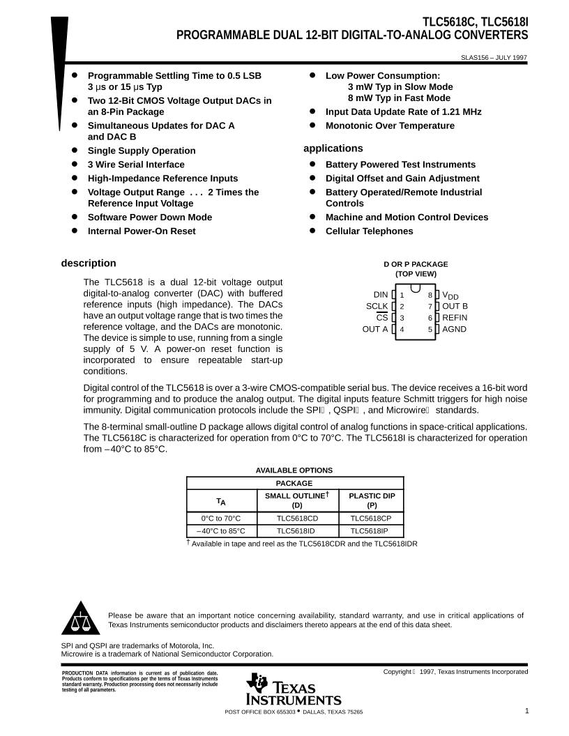
 WMS仓库系统