sp6012.pdf
- 文件大小: 222.88KB
- 文件类型: pdf
- 上传日期: 2025-08-23
- 下载次数: 0
概要信息:
2010/01/ 05 Ver.2
Page 1
SP6012
Synchronous Rectifier Driver
DESCRIPTION APPLICATIONS
The fundamental of SP6012 synchronous
rectifier (SR) driver IC is based on our U.S.
patented methods that utilize the principle of
“prediction” logic circuit. The IC deliberates
previous cycle timing to control the SR in
present cycle by “predictive” algorithm that
makes adjustments to the turn-off time, in order
to achieve maximum efficiency and avoid
cross-conduction at the same time. It also
maintains the MOSFET’s body diode conduction
at minimum level. The SP6012 is capable to
adapt in almost all existing forward converters
with few adjustments considered necessary.
• Servers & workstations
• Storage area network power supplies
• Telecommunication converters
• Embedded systems
• Industrial & commercial systems using high
current processors
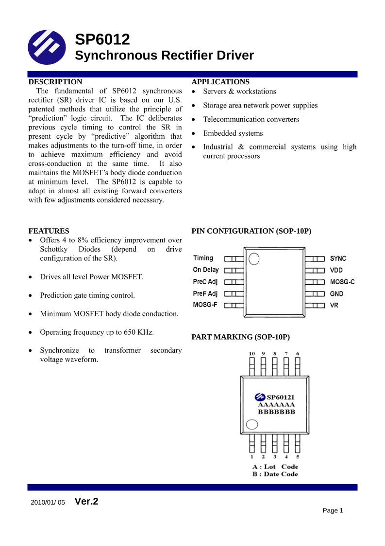
FEATURES PIN CONFIGURATION (SOP-10P)
PART MARKING (SOP-10P)
• Offers 4 to 8% efficiency improvement over
Schottky Diodes (depend on drive
configuration of the SR).
• Drives all level Power MOSFET.
• Prediction gate timing control.
• Minimum MOSFET body diode conduction.
• Operating frequency up to 650 KHz.
• Synchronize to transformer secondary
voltage waveform.
2010/01/ 05 Ver.2
Page 2
SP6012
Synchronous Rectifier Driver
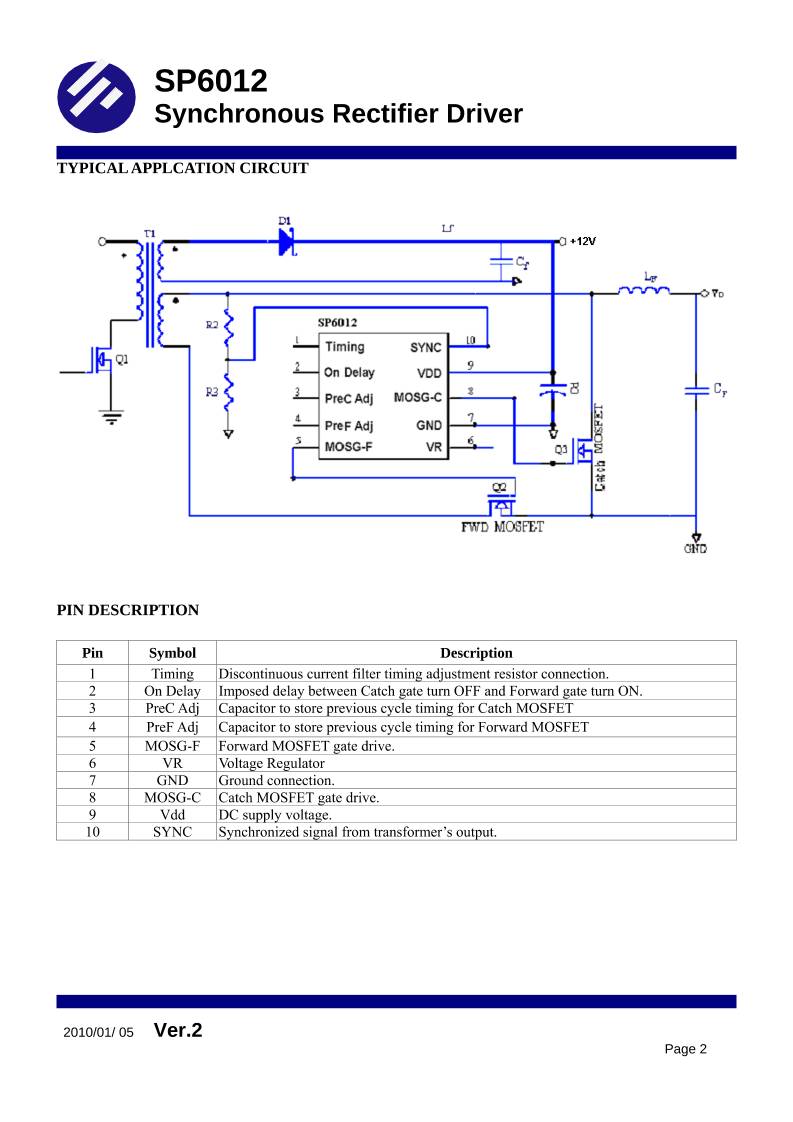
TYPICAL APPLCATION CIRCUIT
PIN DESCRIPTION
Pin Symbol Description
1 Timing Discontinuous current filter timing adjustment resistor connection.
2 On Delay Imposed delay between Catch gate turn OFF and Forward gate turn ON.
3 PreC Adj Capacitor to store previous cycle timing for Catch MOSFET
4 PreF Adj Capacitor to store previous cycle timing for Forward MOSFET
5 MOSG-F Forward MOSFET gate drive.
6 VR Voltage Regulator
7 GND Ground connection.
8 MOSG-C Catch MOSFET gate drive.
9 Vdd DC supply voltage.
10 SYNC Synchronized signal from transformer’s output.
2010/01/ 05 Ver.2
Page 3
SP6012
Synchronous Rectifier Driver
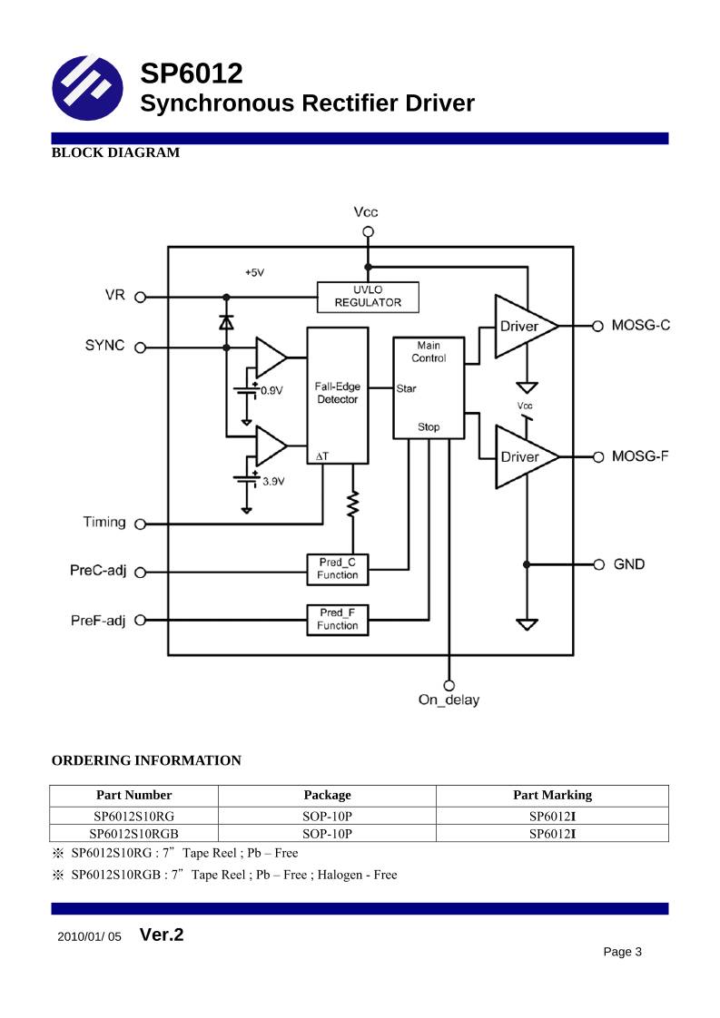
BLOCK DIAGRAM
ORDERING INFORMATION
Part Number Package Part Marking
SP6012S10RG SOP-10P SP6012I
SP6012S10RGB SOP-10P SP6012I
※ SP6012S10RG : 7"Tape Reel ; Pb – Free
※ SP6012S10RGB : 7"Tape Reel ; Pb – Free ; Halogen - Free
2010/01/ 05 Ver.2
Page 4
SP6012
Synchronous Rectifier Driver
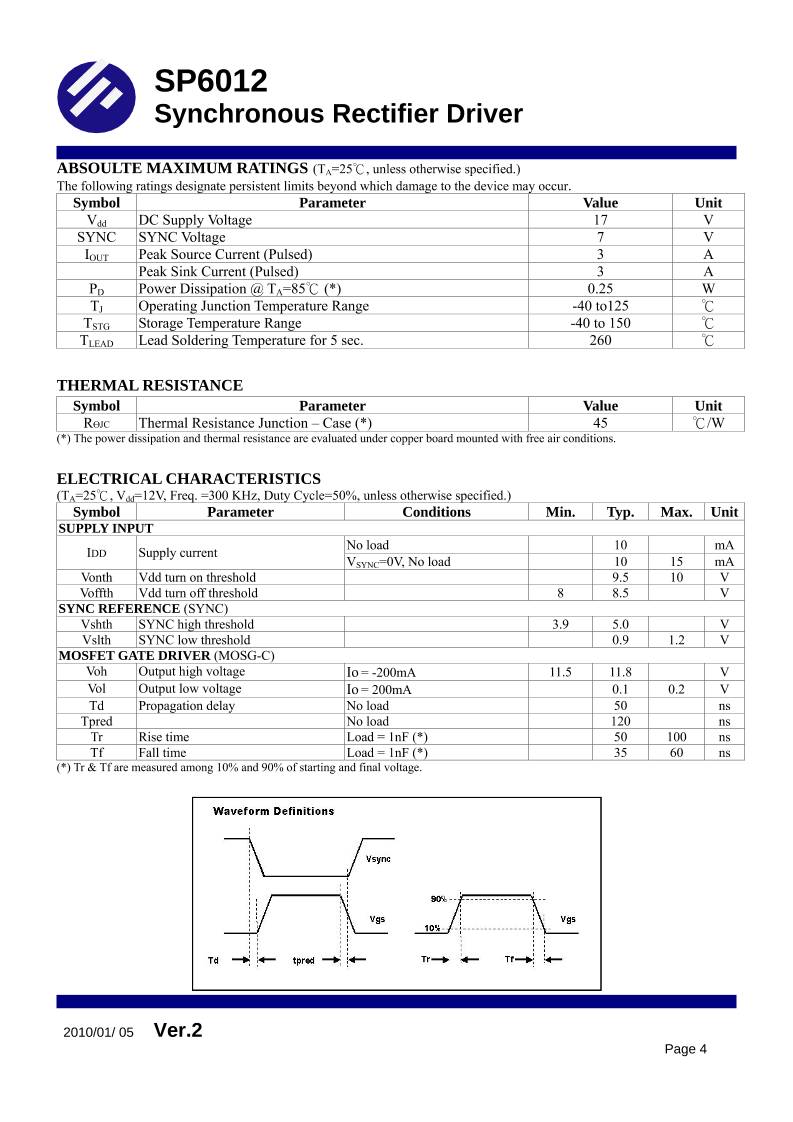
ABSOULTE MAXIMUM RATINGS (TA=25 , unless otherwise specified.)℃
The following ratings designate persistent limits beyond which damage to the device may occur.
Symbol Parameter Value Unit
Vdd DC Supply Voltage 17 V
SYNC SYNC Voltage 7 V
IOUT Peak Source Current (Pulsed) 3 A
Peak Sink Current (Pulsed) 3 A
PD Power Dissipation @ TA=85 (*)℃ 0.25 W
TJ Operating Junction Temperature Range -40 to125 ℃
TSTG Storage Temperature Range -40 to 150 ℃
TLEAD Lead Soldering Temperature for 5 sec. 260 ℃
THERMAL RESISTANCE
Symbol Parameter Value Unit
RӨJC Thermal Resistance Junction – Case (*) 45 /W℃
(*) The power dissipation and thermal resistance are evaluated under copper board mounted with free air conditions.
ELECTRICAL CHARACTERISTICS
(TA=25 , V℃ dd=12V, Freq. =300 KHz, Duty Cycle=50%, unless otherwise specified.)
Symbol Parameter Conditions Min. Typ. Max. Unit
SUPPLY INPUT
No load 10 mAIDD Supply current
VSYNC=0V, No load 10 15 mA
Vonth Vdd turn on threshold 9.5 10 V
Voffth Vdd turn off threshold 8 8.5 V
SYNC REFERENCE (SYNC)
Vshth SYNC high threshold 3.9 5.0 V
Vslth SYNC low threshold 0.9 1.2 V
MOSFET GATE DRIVER (MOSG-C)
Voh Output high voltage Io = -200mA 11.5 11.8 V
Vol Output low voltage Io = 200mA 0.1 0.2 V
Td Propagation delay No load 50 ns
Tpred No load 120 ns
Tr Rise time Load = 1nF (*) 50 100 ns
Tf Fall time Load = 1nF (*) 35 60 ns
(*) Tr & Tf are measured among 10% and 90% of starting and final voltage.
2010/01/ 05 Ver.2
Page 5
SP6012
Synchronous Rectifier Driver
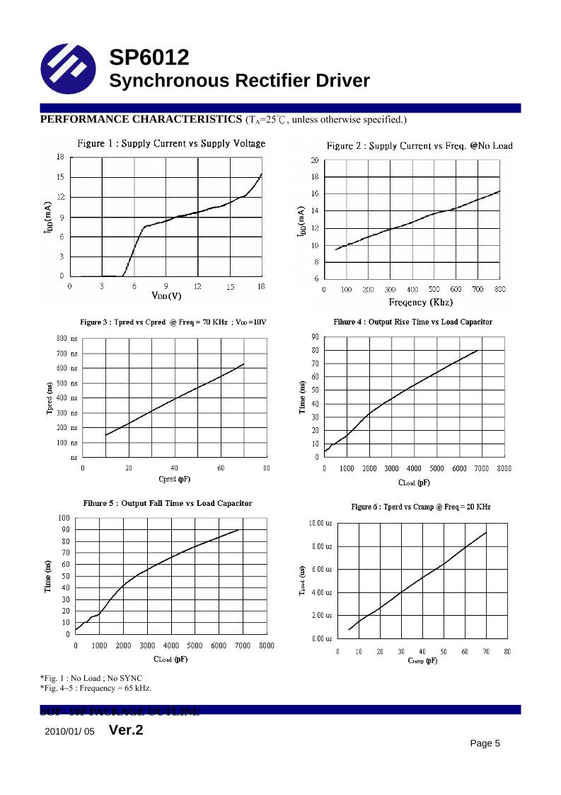
PERFORMANCE CHARACTERISTICS (TA=25 , unless otherwise specified.)℃
*Fig. 1 : No Load ; No SYNC
*Fig. 4~5 : Frequency = 65 kHz.
SOP- 10P PACKAGE OUTLINE
2010/01/ 05 Ver.2
Page 6
SP6012
Synchronous Rectifier Driver
2010/01/ 05 Ver.2
Page 7
SP6012
Synchronous Rectifier Driver
Information provided is alleged to be exact and consistent. SYNC Power Corporation presumes no responsibility for the
penalties of use of such information or for any violation of patents or other rights of third parties that may result from its use.
No license is granted by allegation or otherwise under any patent or patent rights of SYNC Power Corporation. Conditions
mentioned in this publication are subject to change without notice. This publication surpasses and replaces all information
previously supplied. SYNC Power Corporation products are not authorized for use as critical components in life support
devices or systems without express written approval of SYNC Power Corporation.
©The SYNC Power logo is a registered trademark of SYNC Power Corporation
©2004 SYNC Power Corporation – Printed in Taiwan – All Rights Reserved
SYNC Power Corporation
7F-2, No.3-1, Park Street
NanKang District (NKSP), Taipei, Taiwan, 115, R.O.C
Phone: 886-2-2655-8178
Fax: 886-2-2655-8468
http://www.syncpower.com高速下载:
点击后进入安全下载页,再进行实际下载。下载链接有效期 24 小时,过期会自动刷新。
 WMS仓库系统