概要信息:
Electrical Specifications Subject to Change
LT8705
1
8705p
For more information www.linear.com/8705
TYPICAL APPLICATION
FEATURES DESCRIPTION
80V VIN and VOUT
Synchronous 4-Switch Buck-
Boost DC/DC Controller
The LT®8705 is a high performance buck-boost switch-
ing regulator controller that operates from input voltages
above, below or equal to the output voltage. The part has
integrated input current, input voltage, output current
and output voltage feedback loops. With a wide 2.8V to
80V input and 1.3V to 80V output range, the LT8705 is
compatible with most solar, automotive, telecom and
battery-powered systems.
The operating mode of the controller is determined
through the MODE pin. The MODE pin can select among
discontinuous mode, forced continuous mode and Burst
Mode® operation. The LT8705 also features programmable
UVLO and switching currents, along with input and output
current monitoring with programmable maximum levels.
APPLICATIONS L, LT, LTC, LTM, Linear Technology, Burst Mode, µModule and the Linear logo are registered
trademarks of Linear Technology Corporation. All other trademarks are the property of their
respective owners.
n Single Inductor Allows VIN Above, Below, or Equal
to Regulated VOUT
n VIN Range 2.8V (Need EXTVCC > 6.4V) to 80V
n VOUT Range: 1.3V to 80V
n Quad N-Channel MOSFET Gate Drivers
n Synchronous Rectification: Up to 98% Efficiency
n Input and Output Current Monitor Pins
n Synchronizable Fixed Frequency: 100kHz to 400kHz
n Integrated Input Current, Input Voltage, Output
Current and Output Voltage Feedback Loops
n Clock Output Usable To Monitor Die Temperature
n Available in 38-Lead (5mm × 7mm) QFN and TSSOP
Packages with the TSSOP Modified for Improved
High Voltage Operation
n High Voltage Buck-Boost Converters
n Input or Output Current Limited Converters
Telecom Voltage Stabilizer
8705 TA01
CSPOUT
CSNOUT
EXTVCC
FBOUT
INTVCC
GATEVCC
SRVO_FBIN
SRVO_FBOUT
SRVO_IIN
SRVO_IOUT
IMON_IN
IMON_OUTSYNCCLKOUTVC
56.2k
202kHz
CSNIN
TG1 BOOST1
0.22µF 0.22µF
TO
DIODE
TO
DIODE
M2
M1
×2
22µH
4.7µF
×4
M4
M3
×2
1nF
1nF
SW1 BG1 CSP CSN
LT8705
GND BG2 SW2 BOOST2
VOUT
48V
5A
VIN
36V TO
80V
TG2
CSPIN
VIN
SHDN
SWEN
LDO33
MODE
FBIN
RT
SS
3.3nF220pF
215k
71.5k
20k
1µF
1µF
4.7µF
10k
392k
220µF
×2
4.7µF
×6
4Ω
4.7µF
TO
BOOST1
4.7µF
2Ω
×2 2Ω
×2
10mΩ
+
220µF
×2
+
TO
BOOST2
100k
10Ω
10Ω
VIN (V)
30
EF
FI
CI
EN
CY
(%
)
POW
ER LOSS (W
)
90
95
70
8705 TA01b
85
80 0
40 50 60 80
VOUT = 48V
ILOAD = 2A
100 6
5
4
3
2
1
Efficiency and Power Loss
LT8705
2
8705p
For more information www.linear.com/8705
PIN CONFIGURATION
ABSOLUTE MAXIMUM RATINGS
VCSP-VCSN, VCSPIN-VCSNIN,
VCSPOUT-VCSNOUT...................................... –0.3V to 0.3V
SS, CLKOUT, CSP, CSN Voltage ................... –0.3V to 3V
VC Voltage (Note 2) ................................... –0.3V to 2.2V
RT, LDO33, FBOUT Voltage .......................... –0.3V to 5V
IMON_IN, IMON_OUT Voltage ..................... –0.3V to 5V
SYNC Voltage ............................................ –0.3V to 5.5V
INTVCC, GATEVCC Voltage ............................ –0.3V to 7V
VBOOST1-VSW1, VBOOST2-VSW2 ..................... –0.3V to 7V
SWEN, MODE Voltage .................................. –0.3V to 7V
SRVO_FBIN, SRVO_FBOUT Voltage ........... –0.3V to 30V
SRVO_IIN, SRVO_IOUT Voltage ................. –0.3V to 30V
(Note 1)
FBIN, SHDN Voltage ................................... –0.3V to 30V
CSNIN, CSPIN, CSPOUT, CSNOUT Voltage ..–0.3V to 80V
VIN, EXTVCC Voltage .................................. –0.3V to 80V
SW1, SW2 Voltage ......................................81V (Note 7)
BOOST1, BOOST2 Voltage ......................... –0.3V to 87V
BG1, BG2, TG1, TG2 ........................................... (Note 6)
Operating Junction Temperature Range
LT8705E (Notes 1, 3) ......................... –40°C to 125°C
LT8705I (Notes 1, 3) .......................... –40°C to 125°C
Storage Temperature Range .................. –65°C to 150°C
Lead Temperature (Soldering, 10 sec)
FE Package ....................................................... 300°C
13 14 15 16
TOP VIEW
39
GND
UHF PACKAGE
38-LEAD (5mm × 7mm) PLASTIC QFN
17 18 19
38 37 36 35 34 33 32
24
25
26
27
28
29
30
31
8
7
6
5
4
3
2
1SHDN
CSN
CSP
LDO33
FBIN
FBOUT
IMON_OUT
VC
SS
CLKOUT
SYNC
RT
CSPOUT
CSNOUT
EXTVCC
SRVO_FBOUT
SRVO_IOUT
SRVO_IIN
SRVO_FBIN
NC
BOOST1
TG1
SW1
NC
IM
ON
_I
N
M
OD
E
SW
EN
IN
TV
CC
V I
N
CS
PI
N
CS
NI
N
GN
D
BG
1
GA
TE
V C
C
BG
2
BO
OS
T2 TG
2
SW
2
23
22
21
20
9
10
11
12
TJMAX = 125°C, θJA = 34°C/W
EXPOSED PAD (PIN 39) IS GND, MUST BE SOLDERED TO PCB
1
2
3
4
5
6
7
8
9
10
11
12
13
14
15
16
17
18
19
TOP VIEW
FE PACKAGE
VARIATION: FE38(31)
38-LEAD PLASTIC TSSOP
38
37
36
34
32
30
28
26
24
22
21
20
39
GND
INTVCC
MODE
IMON_IN
SHDN
CSN
CSP
LDO33
FBIN
FBOUT
IMON_OUT
VC
SS
CLKOUT
SYNC
RT
GND
BG1
GATEVCC
BG2
VIN
CSPIN
CSNIN
CSPOUT
CSNOUT
EXTVCC
BOOST1
TG1
SW1
SW2
TG2
BOOST2
TJMAX = 125°C, θJA = 25°C/W
EXPOSED PAD (PIN 39) IS GND, MUST BE SOLDERED TO PCB
LT8705
3
8705p
For more information www.linear.com/8705
ELECTRICAL CHARACTERISTICS
PARAMETER CONDITIONS MIN TYP MAX UNITS
Voltage Supplies and Regulators
VIN Operating Voltage Range EXTVCC = 0V
EXTVCC = 7.5V
l
l
5.5
2.8
80
80
V
V
VIN Quiescent Current Not Switching, VEXTVCC = 0 2.65 4.2 mA
VIN Quiescent Current in Shutdown VSHDN = 0V 0 1 µA
EXTVCC Switchover Voltage IINTVCC = 20mA, VEXTVCC Rising l 6.15 6.4 6.6 V
EXTVCC Switchover Hysteresis 0.18 V
INTVCC Current Limit Maximum Current Draw from INTVCC and LDO33
Pins Combined. Regulated from VIN or EXTVCC (12V)
INTVCC = 5.25V
INTVCC = 4.5V
l
l
90
28
127
42
165
55
mA
mA
INTVCC Voltage Regulated from VIN, IINTVCC = 20mA
Regulated from EXTVCC (12V), IINTVCC = 20mA
l
l
6.15
6.15
6.35
6.35
6.55
6.55
V
V
INTVCC Load Regulation IINTVCC = 0mA to 50mA –0.5 –1.5 %
INTVCC, GATEVCC Undervoltage Lockout INTVCC Falling, GATEVCC Connected to INTVCC l 4.45 4.65 4.85 V
INTVCC, GATEVCC Undervoltage Lockout Hysteresis GATEVCC Connected to INTVCC 160 mV
INTVCC Regulator Dropout Voltage VIN-VINTVCC, IINTVCC = 20mA 245 mV
LDO33 Pin Voltage 5mA from LDO33 Pin l 3.23 3.295 3.35 V
LDO33 Pin Load Regulation ILDO33 = 0.1mA to 5mA –0.25 –1 %
LDO33 Pin Current Limit l 12 17.25 22 mA
LDO33 Pin Undervoltage Lockout LDO33 Falling 2.96 3.04 3.12 V
LDO33 Pin Undervoltage Lockout Hysteresis 35 mV
Switching Regulator Control
Maximum Current Sense Threshold (VCSP – VCSN) Boost Mode, Minimum M3 Switch Duty Cycle l 102 117 132 mV
Maximum Current Sense Threshold (VCSN – VCSP) Buck Mode, Minimum M2 Switch Duty Cycle l 69 86 102 mV
Gain from VC to Maximum Current Sense Voltage
(VCSP-VCSN) (A5 in the Block Diagram)
Boost Mode
Buck Mode
150
–150
mV/V
mV/V
SHDN Input Voltage High SHDN Rising to Enable the Device l 1.184 1.234 1.284 V
SHDN Input Voltage High Hysteresis 50 mV
SHDN Input Voltage Low Device Disabled, Low Quiescent Current l 0.35 V
The l denotes the specifications which apply over the full operating
temperature range, otherwise specifications are at TA = 25°C. VIN = 12V, SHDN = 3V unless otherwise noted. (Note 3)
ORDER INFORMATION
LEAD FREE FINISH TAPE AND REEL PART MARKING* PACKAGE DESCRIPTION TEMPERATURE RANGE
LT8705EUHF#PBF LT8705EUHF#TRPBF 8705 38-Lead (5mm × 7mm) Plastic QFN –40°C to 125°C
LT8705IUHF#PBF LT8705IUHF#TRPBF 8705 38-Lead (5mm × 7mm) Plastic QFN –40°C to 125°C
LT8705EFE#PBF LT8705EFE#TRPBF LT8705FE 38-Lead Plastic TSSOP –40°C to 125°C
LT8705IFE#PBF LT8705IFE#TRPBF LT8705FE 38-Lead Plastic TSSOP –40°C to 125°C
Consult LTC Marketing for parts specified with wider operating temperature ranges. *The temperature grade is identified by a label on the shipping container.
For more information on lead free part marking, go to: http://www.linear.com/leadfree/
For more information on tape and reel specifications, go to: http://www.linear.com/tapeandreel/
LT8705
4
8705p
For more information www.linear.com/8705
PARAMETER CONDITIONS MIN TYP MAX UNITS
SHDN Pin Bias Current VSHDN = 3V
VSHDN = 12V
0
11
1
22
µA
µA
SWEN Rising Threshold Voltage (Note 5) l 1.156 1.206 1.256 V
SWEN Threshold Voltage Hysteresis (Note 5) 22 mV
MODE Pin Forced Continuous Mode Threshold l 0.4 V
MODE Pin Burst Mode Range l 1.0 1.7 V
MODE Pin Discontinuous Mode Threshold l 2.3 V
Soft-Start Charging Current VSS = 0.5V 13 19 25 µA
Soft-Start Discharge Current VSS = 0.5V 9.5 µA
Voltage Regulator Loops (Refer to Block Diagram to Locate Amplifiers)
Regulation Voltage for FBOUT VC = 1.2V l 1.193 1.207 1.217 V
Regulation Voltage for FBIN VC = 1.2V l 1.187 1.205 1.220 V
Line Regulation for FBOUT and FBIN Error Amp Reference
Voltage
VIN = 12V to 80V 0.002 0.005 %/V
FBOUT Pin Bias Current Current Out of Pin 15 nA
FBOUT Error Amp EA4 gm 315 µmho
FBOUT Error Amp EA4 Voltage Gain 220 V/V
FBIN Pin Bias Current Current Out of Pin 10 nA
FBIN Error Amp EA3 gm 130 µmho
FBIN Error Amp EA3 Voltage Gain 90 V/V
SRVO_FBIN Activation Threshold (Note 5) (VFBIN Falling) – (Regulation Voltage for FBIN),
VFBOUT = VIMON_IN = VIMON_OUT = 0V
56 72 89 mV
SRVO_FBIN Activation Threshold Hysteresis (Note 5) VFBOUT = VIMON_IN = VIMON_OUT = 0V 33 mV
SRVO_FBOUT Activation Threshold (Note 5) (VFBOUT Rising) – (Regulation Voltage for FBOUT),
VFBIN = 3V, VIMON_IN = VIMON_OUT = 0V
–37 –29 –21 mV
SRVO_FBOUT Activation Threshold Hysteresis (Note 5) VFBIN = 3V, VIMON_IN = 0V, VIMON_OUT = 0V 15 mV
SRVO_FBIN, SRVO_FBOUT Low Voltage (Note 5) I = 100μA l 110 330 mV
SRVO_FBIN, SRVO_FBOUT Leakage Current (Note 5) VSRVO_FBIN = VSRVO_FBOUT = 2.5V l 0 1 µA
Current Regulation Loops (Refer to Block Diagram to Locate Amplifiers)
Regulation Voltages for IMON_IN and IMON_OUT VC = 1.2V l 1.191 1.208 1.223 V
Line Regulation for IMON_IN and IMON_OUT Error Amp
Reference Voltage
VIN = 12V to 80V 0.002 0.005 %/V
CSPIN, CSNIN Bias Current BOOST Capacitor Charge Control Block Not Active
ICSPIN + ICSNIN, VCSPIN = VCSNIN = 12V
31
µA
CSPIN, CSNIN Common Mode Operating Voltage Range l 1.5 80 V
CSPIN, CSNIN Differential Operating Voltage Range l –100 100 mV
VCSPIN-CSNIN to IMON_IN Amplifier A7 gm VCSPIN – VCSNIN = 50mV, VCSPIN = 5.025V
l
0.95
0.94
1
1
1.05
1.06
mmho
mmho
IMON_IN Maximum Output Current l 100 µA
IMON_IN Overvoltage Threshold l 1.55 1.61 1.67 V
IMON_IN Error Amp EA2 gm 185 µmho
IMON_IN Error Amp EA2 Voltage Gain 130 V/V
ELECTRICAL CHARACTERISTICS The l denotes the specifications which apply over the full operating
temperature range, otherwise specifications are at TA = 25°C. VIN = 12V, SHDN = 3V unless otherwise noted. (Note 3)
LT8705
5
8705p
For more information www.linear.com/8705
PARAMETER CONDITIONS MIN TYP MAX UNITS
CSPOUT, CSNOUT Bias Current BOOST Capacitor Charge Control Block Not Active
ICSPOUT + ICSNOUT, VCSPOUT = VCSNOUT = 12V
ICSPOUT + ICSNOUT, VCSPOUT = VCSNOUT = 1.5V
45
4
µA
µA
CSPOUT, CSNOUT Common Mode Operating Voltage Range l 0 80 V
CSPOUT, CSNOUT Differential Mode Operating Voltage Range l –100 100 mV
VCSPOUT-CSNOUT to IMON_OUT Amplifier A6 gm VCSPOUT – VCSNOUT = 50mV, VCSPOUT = 5.052V
VCSPOUT – VCSNOUT = 50mV, VCSPOUT = 5.025V
VCSPOUT – VCSNOUT = 5mV, VCSPOUT = 5.0025V
VCSPOUT – VCSNOUT = 5mV, VCSPOUT = 5.0025V
l
l
0.95
0.94
0.65
0.55
1
1
1
1
1.05
1.085
1.35
1.6
mmho
mmho
mmho
mmho
IMON_OUT Maximum Output Current l 100 µA
IMON_OUT Overvoltage Threshold l 1.55 1.61 1.67 V
IMON_OUT Error Amp EA1 gm 185 µmho
IMON_OUT Error Amp EA1 Voltage Gain 130 V/V
SRVO_IIN Activation Threshold (Note 5) (VIMON_IN Rising) – (Regulation Voltage for
IMON_IN), VFBIN = 3V, VFBOUT = 0V, VIMON_OUT = 0V
–60 –49 –37 mV
SRVO_IIN Activation Threshold Hysteresis (Note 5) VFBIN = 3V, VFBOUT = 0V, VIMON_OUT = 0V 22 mV
SRVO_IOUT Activation Threshold (Note 5) (VIMON_OUT Rising) – (Regulation Voltage for IMON_
OUT), VFBIN = 3V, VFBOUT = 0V, VIMON_IN = 0V
–62 –51 –39 mV
SRVO_IOUT Activation Threshold Hystersis (Note 5) VFBIN = 3V, VFBOUT = 0V, VIMON_IN = 0V 22 mV
SRVO_IIN, SRVO_IOUT Low Voltage (Note 5) I = 100μA l 110 330 mV
SRVO_IIN, SRVO_IOUT Leakage Current (Note 5) VSRVO_IIN = VSRVO_IOUT = 2.5V l 0 1 µA
NMOS Gate Drivers
TG1, TG2 Rise Time CLOAD = 3300pF (Note 4) 20 ns
TG1, TG2 Fall Time CLOAD = 3300pF (Note 4) 20 ns
BG1, BG2 Rise Time CLOAD = 3300pF (Note 4) 20 ns
BG1, BG2 Fall Time CLOAD = 3300pF (Note 4) 20 ns
TG1 Off to BG1 On Delay CLOAD = 3300pF Each Driver 100 ns
BG1 Off to TG1 On Delay CLOAD = 3300pF Each Driver 80 ns
TG2 Off to BG2 On Delay CLOAD = 3300pF Each Driver 100 ns
BG2 Off to TG2 On Delay CLOAD = 3300pF Each Driver 80 ns
Minimum On-Time for Main Switch in Boost Operation
(tON(M3,MIN))
Switch M3, CLOAD = 3300pF 265 ns
Minimum On-Time for Synchronous Switch in Buck
Operation (tON(M2,MIN))
Switch M2, CLOAD = 3300pF 260 ns
Minimum Off-Time for Main Switch in Steady-State Boost
Operation
Switch M3, CLOAD = 3300pF 245 ns
Minimum Off-Time for Synchronous Switch in
Steady-State Buck Operation
Switch M2, CLOAD = 3300pF 245 ns
Oscillator
Switch Frequency Range SYNCing or Free Running 100 400 kHz
Switching Frequency, fOSC RT = 365k
RT = 215k
RT = 124K
l
l
l
102
170
310
120
202
350
142
235
400
kHz
kHz
kHz
ELECTRICAL CHARACTERISTICS The l denotes the specifications which apply over the full operating
temperature range, otherwise specifications are at TA = 25°C. VIN = 12V, SHDN = 3V unless otherwise noted. (Note 2)
LT8705
6
8705p
For more information www.linear.com/8705
Note 1: Stresses beyond those listed under Absolute Maximum Ratings
may cause permanent damage to the device. Exposure to any Absolute
Maximum Rating condition for extended periods may affect device
reliability and lifetime.
Note 2: Do not force voltage on the VC pin.
Note 3: The LT8705E is guaranteed to meet performance specifications
from 0°C to 125°C junction temperature. Specifications over the –40°C
to 125°C operating junction temperature range are assured by design,
characterization and correlation with statistical process controls. The
LT8705I is guaranteed over the full –40°C to 125°C junction temperature
range.
Note 4: Rise and fall times are measured using 10% and 90% levels. Delay
times are measured using 50% levels.
Note 5: This specification not applicable in the FE38 package.
Note 6: Do not apply a voltage or current source to these pins. They must
be connected to capacitive loads only, otherwise permanent damage may
occur.
Note 7: Negative voltages on the SW1 and SW2 pins are limited, in an
application, by the body diodes of the external NMOS devices, M2 and
M3, or parallel Schottky diodes when present. The SW1 and SW2 pins
are tolerant of these negative voltages in excess of one diode drop below
ground, guaranteed by design.
PARAMETER CONDITIONS MIN TYP MAX UNITS
SYNC High Level for Synchronization l 1.3 V
SYNC Low Level for Synchronization l 0.5 V
SYNC Clock Pulse Duty Cycle VSYNC = 0V to 2V 20 80 %
Recommended Minimum SYNC Ratio fSYNC/fOSC 3/4
CLKOUT Output Voltage High 1mA Out of CLKOUT Pin 2.3 2.45 2.55 V
CLKOUT Output Voltage Low 1mA Into CLKOUT Pin 25 100 mV
CLKOUT Duty Cycle TJ = –40°C
TJ = 25°C
TJ = 125°C
21.4
42.5
75
%
%
%
CLKOUT Rise Time CLOAD = 200pF 30 ns
CLKOUT Fall Time CLOAD = 200pF 25 ns
CLKOUT Phase Delay SYNC Rising to CLKOUT Rising, fOSC = 100kHz l 160 180 200 Deg
ELECTRICAL CHARACTERISTICS The l denotes the specifications which apply over the full operating
temperature range, otherwise specifications are at TA = 25°C. VIN = 12V, SHDN = 3V unless otherwise noted. (Note 3)
LT8705
7
8705p
For more information www.linear.com/8705
TYPICAL PERFORMANCE CHARACTERISTICS
FBOUT Voltages (Five Parts)Feedback Voltages Oscillator Frequency
Maximum Inductor Current Sense
Voltage vs Duty Cycle
Inductor Current Sense Voltage at
Minimum Duty Cycle
Efficiency vs Output Current
(Boost Region-Figure 14)
Efficiency vs Output Current
(Buck-Boost Region-Figure 14)
Efficiency vs Output Current
(Buck Region-Figure 14)
LOAD CURRENT (mA)
10
0
EF
FI
CI
EN
CY
(%
)
20
30
40
50
60
70
100 1000
8705 G01
80
90
100
VIN = 36V
VOUT = 48V
10
10000
BURST
CCM
DCM
LOAD CURRENT (mA)
10
0
EF
FI
CI
EN
CY
(%
)
20
30
40
50
60
70
100 1000
8705 G02
80
90
100
VIN = 48V
VOUT = 48V
10
10000
BURST
CCM
DCM
LOAD CURRENT (mA)
10
0
EF
FI
CI
EN
CY
(%
)
20
30
40
50
60
70
100 1000
8705 G03
80
90
100
VIN = 72V
VOUT = 48V
10
10000
BURST
CCM
DCM
TEMPERATURE (°C)
–55
1.17
PI
N
VO
LT
AG
E
(V
)
1.18
1.19
1.20
1.21
–5 45 95 145
8705 G04
1.22
1.23
–30 20 70 120
IMON_OUT
IMON_IN
FBOUT
FBIN
VC = 1.2V
TEMPERATURE (°C)
–50
FB
OU
T
VO
LT
AG
E
(V
)
1.21
1.22
1.23
25 75
8795 G05
1.20
1.19
–25 0 50 100 150125
1.18
1.17
VC = 1.2V
TEMPERATURE (°C)
–40
FR
EQ
UE
NC
Y
(k
Hz
)
200
300
120
8705 G06
100
0
0 40 80–20 20 60 100
400
RT = 124k
RT = 215k
RT = 365k150
250
50
350
M2 OR M3 DUTY CYCLE (%)
0
100
120
140
80
8705 G07
80
60
20 40 60 100
40
20
0
|C
SP
-C
SN
| (
m
V)
BUCK REGION
BOOST REGION
VC (V)
0.5
–80
CS
N-
CS
P
(m
V)
CSP-CSN (m
V)
–40
–20
0
20
40
60
1 1.5
8705 G08
80
100
120
BUCK REGION
BOOST REGION
–60
–80
–40
–20
0
20
40
60
80
100
120
–60
2
Maximum Inductor Current Sense
Voltage at Minimum Duty Cycle
TEMPERATURE (°C)
–40
0
|C
SP
-C
SN
| (
m
V)
20
40
60
80
100
120
0 40 80–20 20 60 100 120
8705 G09
BOOST REGION
BUCK REGION
TA = 25°C unless otherwise specified.
LT8705
8
8705p
For more information www.linear.com/8705
TYPICAL PERFORMANCE CHARACTERISTICS
IMON Output Currents
CLKOUT Duty Cycle
LDO33 Pin Regulation
(ILDO33 = 1mA)
SHDN and SWEN Pin Thresholds
vs Temperature
INTVCC Line Regulation
(EXTVCC = 0V)
INTVCC Line Regulation
(VIN = 12V)
Maximum VC vs SS
Minimum Inductor Current Sense
Voltage in Forced Continuous Mode
VIN Supply Current vs Voltage
(Not Switching)
M2 OR M3 DUTY CYCLE (%)
0
–40
–20
0
80
8705 G10
–60
–80
20 40 60 100
–100
–120
–140
–|
CS
P-
CS
N|
(m
V)
BUCK REGION
BOOST REGION
VIN (V)
4
4.0
IN
TV
CC
(V
)
4.5
5.0
5.5
6.0
8 12 16 20
8705 G11
6.5
7.0
6 10 14 18
EXTVCC (V)
4
5.5
IN
TV
CC
(V
)
6.0
6.5
7.0
6 8
8705 G12
10 12
EXTVCC RISING
EXTVCC FALLING
SS (V)
0
0
M
AX
IM
UM
V
C
(V
)
0.2
0.6
0.8
1.0
2.0
1.4
0.4 0.8 1.0 1.2
8705 G13
0.4
1.6
1.8
1.2
0.2 0.6 1.4
BOOST AND
BUCK-BOOST REGIONS
BUCK
REGION
TJ = 25°C
VIN (V)
5
I IN
(m
A) 2.0
2.5
3.0
65 7535 45 55
8705 G14
1.5
1.0
15 25
0.5
0
3.5
GATEVCC CONNECTED TO INTVCC
125°C
25°C
–40°C
CSPIN-CSNIN (mV)
CSPOUT-CSNOUT (mV)
–100
–25
IM
ON
_O
UT
, I
M
ON
_I
N
(µ
A)
0
50
75
100
100
200
8705 G15
25
0–50 15050 200
125
150
175
TEMPERATURE (°C)
–50
DU
TY
C
YC
LE
(%
)
60
80
100
25 75 150
8705 G16
40
20
0
–25 0 50 100 125
INTVCC (V)
2.5
LD
O
(V
)
2.5
3.0
6
8705 G17
2.0
1.5
3 43.5 4.5 5 5.5
3.5
125°C
25°C
–40°C
TEMPERATURE (°C)
–55
PI
N
TH
RE
SH
OL
D
VO
LT
AG
E
(V
)
1.22
1.26
1.30
125
8705 G18
1.18
1.14
1.20
1.24
1.28
1.16
1.12
1.10
–15 25 65 85–35 1455 45 105
RISING
FALLING
SHDN
SWEN
TA = 25°C unless otherwise specified.
LT8705
9
8705p
For more information www.linear.com/8705
TYPICAL PERFORMANCE CHARACTERISTICS
Discontinuous Mode (Figure 14)
Forced Continuous Mode
(Figure 14)
Forced Continuous Mode
(Figure 14)
Forced Continuous Mode
(Figure 14)
SHDN and MODE Pin Currents Internal VIN UVLO
SRVO_xx Pin Activation
Thresholds
SRVO_xx Pin Activation Threshold
Hysteresis
PIN VOLTAGE (V)
0
CU
RR
EN
T
IN
TO
P
IN
(µ
A)
10
14
18
24
8705 G19
6
2
8
12
16
4
0
–2
63 129 18 21 2715 30
MODE
SHDN
TEMPERATURE (°C)
–40 –20
0
V I
N
UV
LO
(V
)
0.5
1.0
1.5
2.0
2.5
3.0
0 20 40 60 80 100 120
8705 G20
TEMPERATURE (°C)
–50
V P
IN
-V
RE
GU
LA
TI
ON
V P
IN
A
PP
RO
AC
HI
NG
V
RE
GU
LA
TI
ON
(m
V)
25
75
150
8705 G21
–25
–75
0 50 100–25 25 75 125
125
0
50
–50
100
FBIN
FBOUT
IMON_IN
IMON_OUT
TEMPERATURE (°C)
–50
PI
N
AC
TI
VA
TI
ON
T
HR
ES
HO
LD
H
YS
TE
RS
IS
(m
V)
30
40
50
25 75 150
8705 G22
20
10
0
–25 0 50 100 125
FBIN
FBOUT
IMON_IN
IMON_OUT
SW1
50V/DIV
SW2
50V/DIV
IL
2A/DIV
5µs/DIVVIN = 72V
VOUT = 48V
8705 G23
SW1
20V/DIV
SW2
20V/DIV
IL
2A/DIV
5µs/DIVVIN = 36V
VOUT = 48V
8705 G24
SW1
20V/DIV
SW2
20V/DIV
IL
2A/DIV
5µs/DIVVIN = 48V
VOUT = 48V
8705 G25
SW1
20V/DIV
SW2
20V/DIV
IL
2A/DIV
5µs/DIVVIN = 72V
VOUT = 48V
8705 G26
TA = 25°C unless otherwise specified.
LT8705
10
8705p
For more information www.linear.com/8705
TYPICAL PERFORMANCE CHARACTERISTICS
Load Step (Figure 14) Load Step (Figure 14)
Load Step (Figure 14)
Line Transient (Figure 14) Line Transient (Figure 14)
Burst Mode Operation (Figure 14) Burst Mode Operation (Figure 14)
VOUT
100mV/DIV
IL
1A/DIV
2ms/DIVVIN = 36V
VOUT = 48V
8705 G27
VOUT
100mV/DIV
IL
5A/DIV
5ms/DIVVIN = 72V
VOUT = 48V
8705 G28
VOUT
500mV/DIV
IL
2A/DIV
500µs/DIVVIN = 36V
VOUT = 48V
LOAD STEP = 1A TO 3A
8705 G29
VOUT500mV/DIV
IL2A/DIV
500µs/DIVVIN = 48VVOUT = 48VLOAD STEP = 1A TO 3A
8705 G30
VOUT
500mV/DIV
IL
2A/DIV
500µs/DIVVIN = 48V
VOUT = 48V
LOAD STEP = 1A TO 3A
8705 G30
VOUT
500mV/DIV
IL
2A/DIV
500µs/DIVVIN = 72V
VOUT = 48V
LOAD STEP = 1A TO 3A
8705 G31
VOUT
0.5V/DIV
VC
0.5V/DIV
VIN
36V TO 72V
IL
2A/DIV
2ms/DIV 8705 G32
VOUT
0.5V/DIV
VC
0.5V/DIV
VIN
72V TO 36V
IL
2A/DIV
2ms/DIV 8705 G33
TA = 25°C unless otherwise specified.
LT8705
11
8705p
For more information www.linear.com/8705
PIN FUNCTIONS
SHDN (Pin 1/Pin 4): Shutdown Pin. Tie high to enable
device. Ground to shut down and reduce quiescent current
to a minimum. Do not float this pin.
CSN (Pin 2/Pin 5): The (–) Input to the Inductor Current
Sense and Reverse-Current Detect Amplifier.
CSP (Pin 3/Pin 6): The (+) Input to the Inductor Current
Sense and Reverse-Current Detect Amplifier. The VC pin
voltage and built-in offsets between CSP and CSN pins, in
conjunction with the RSENSE resistor value, set the current
trip threshold.
LDO33 (Pin 4/Pin7): 3.3V Regulator Output. Bypass this
pin to ground with a minimum 0.1μF ceramic capacitor.
FBIN (Pin 5/Pin 8): Input Feedback Pin. This pin is con-
nected to the input error amplifier input.
FBOUT (Pin 6/Pin 9): Output Feedback Pin. This pin
connects the error amplifier input to an external resistor
divider from the output.
IMON_OUT (Pin 7/Pin 10): Output Current Monitor Pin. The
current out of this pin is proportional to the output current.
See the Operation and Applications Information sections.
VC (Pin 8/Pin 11): Error Amplifier Output Pin. Tie external
compensation network to this pin.
SS (Pin 9/Pin 12): Soft-Start Pin. Place at least 100nF of
capacitance here. Upon start-up, this pin will be charged
by an internal resistor to 2.5V.
CLKOUT (Pin 10/Pin 13): Clock Output Pin. Use this pin to
synchronize one or more compatible switching regulator
ICs to the LT8705. CLKOUT toggles at the same frequency
as the internal oscillator or as the SYNC pin, but is ap-
proximately 180° out of phase. CLKOUT may also be used
as a temperature monitor since the CLKOUT duty cycle
varies linearly with the part’s junction temperature. The
CLKOUT pin can drive capacitive loads up to 200pF.
SYNC (Pin 11/Pin 14): To synchronize the switching fre-
quency to an outside clock, simply drive this pin with a
clock. The high voltage level of the clock needs to exceed
1.3V, and the low level should be less than 0.5V. Drive this
pin to less than 0.5V to revert to the internal free-running
clock. See the Applications Information section for more
information.
(QFN/TSSOP)
RT (Pin 12/Pin 15): Timing Resistor Pin. Adjusts the switch-
ing frequency. Place a resistor from this pin to ground to
set the free-running frequency. Do not float this pin.
BG1, BG2 (Pins 14, 16/Pins 17, 19): Bottom Gate Drive.
Drives the gates of the bottom N-channel MOSFETs be-
tween ground and GATEVCC.
GATEVCC (Pin 15/Pin 18): Power Supply for Gate Drivers.
Must be connected to the INTVCC pin. Do not power from
any other supply. Locally bypass to GND.
BOOST1, BOOST2 (Pins 23, 17/Pins 28, 20): Boosted
Floating Driver Supply. The (+) terminal of the bootstrap
capacitor connects here. The BOOST1 pin swings from a
diode voltage below GATEVCC up to VIN + GATEVCC. The
BOOST2 pin swings from a diode voltage below GATEVCC
up to VOUT + GATEVCC
TG1, TG2 (Pins 22, 18/Pins 26, 21): Top Gate Drive. Drives
the top N-channel MOSFETs with voltage swings equal
to GATEVCC superimposed on the switch node voltages.
SW1, SW2 (Pins 21, 19/Pins 24, 22): Switch Nodes. The
(–) terminals of the bootstrap capacitors connect here.
SRVO_FBIN (Pin 25 QFN Only): Open-Drain Logic Out-
put. This pin is pulled to ground when the input voltage
feedback loop is active.
SRVO_IIN (Pin 26 QFN Only): Open-Drain Logic Output.
The pin is pulled to ground when the input current loop
is active.
SRVO_IOUT (Pin 27 QFN Only): Open-Drain Logic Out-
put. The pin is pulled to ground when the output current
feedback loop is active.
SRVO_FBOUT (Pin 28 QFN Only): Open-Drain Logic Out-
put. This pin is pulled to ground when the output voltage
feedback loop is active.
EXTVCC (Pin 29/Pin 30): External VCC Input. When EXTVCC
exceeds 6.4V (typical), INTVCC will be powered from this
pin. When EXTVCC is lower than 6.22V (typical), INTVCC
will be powered from VIN.
CSNOUT (Pin 30/Pin 32): The (–) Input to the Output Cur-
rent Monitor Amplifier. Connect this pin to VOUT when not
in use. See Applications Information section for proper
use of this pin.
LT8705
12
8705p
For more information www.linear.com/8705
CSPOUT (Pin 31/Pin 34): The (+) Input to the Output
Current Monitor Amplifier. This pin and the CSNOUT pin
measure the voltage across the sense resistor, RSENSE2,
to provide the output current signals. Connect this pin
to VOUT when not in use. See Applications Information
section for proper use of this pin.
CSNIN (Pin 32/Pin 36): The (–) Input to the Input Current
Monitor Amplifier. This pin and the CSPIN pin measure
the voltage across the sense resistor, RSENSE1, to provide
the input current signals. Connect this pin to VIN when not
in use. See Applications Information section for proper
use of this pin.
CSPIN (Pin 33/Pin 37): The (+) Input to the Input Cur-
rent Monitor Amplifier. Connect this pin to VIN when not
in use. See Applications Information section for proper
use of this pin.
VIN (Pin 34/Pin 38): Main Input Supply Pin. It must be
locally bypassed to ground.
INTVCC (Pin 35/Pin 1): Internal 6.35V Regulator Output.
Must be connected to the GATEVCC pin. INTVCC is powered
from EXTVCC when the EXTVCC voltage is higher than
6.4V, otherwise INTVCC is powered from VIN . Bypass this
pin to ground with a minimum 4.7μF ceramic capacitor.
SWEN (Pin 36 QFN Only): Switch Enable Pin. Tie high
to enable switching. Ground to disable switching. Don’t
float this pin. This pin is internally tied to INTVCC in the
TSSOP package.
IMON_IN (Pin 38/Pin 3): Input Current Monitor Pin. The
current out of this pin is proportional to the input current.
See the Operation and Applications Information sections.
MODE (Pin 37/Pin 2): Mode Pin. The voltage applied to
this pin sets the operating mode of the controller. When
the applied voltage is less than 0.4V, the forced continu-
ous current mode is active. When this pin is allowed to
float, Burst Mode operation is active. When the MODE pin
voltage is higher than 2.3V, discontinuous mode is active.
GND (Pin 13, Exposed Pad Pin 39/Pin 16, Exposed Pad
Pin 39): Ground. Tie directly to local ground plane.
PIN FUNCTIONS (QFN/TSSOP)
LT8705
13
8705p
For more information www.linear.com/8705
BLOCK DIAGRAM
Figure 1. Block Diagram
VIN
CSNIN
RSENSE1
RSENSE
RSENSE2
VOUT
VIN
CSN CSP
CSPIN
IMON_IN
MODE
CLKOUT
SYNC
RT
SS
2.5V
EXTVCC
RSHDN2
INTVCC
BOOST1
TG1 CB1
M1
M2
M3
D1
(OPT)
D2
(OPT)
M4
CB2
DB2
DB1
SW1
GATEVCC
BG1
GND
BG2
SW2
TG2
BOOST2
CSPOUT
CSNOUT
IMON_OUT
FBIN
RFBIN1
RFBOUT1
RFBOUT2
RFBIN2
FBOUT
VC
SWEN
OSC
FAULT_INT
STARTUP
AND FAULT
LOGIC
–
+
8705 F01
A7
SHDN
1.234V –
+
–
+
A5
UV_INTVCC OT OI_IN OI_OUT
UV_VINUV_LDO33 UV_GATEVCC
6.35V
LDO
REG
6.35V
LDO
REG
3.3V
LDO
REG
6.4V
EN EN INTERNAL
SUPPLY2
INTERNAL
SUPPLY1
VIN–
+
–
+
–
+
BUCK
LOGIC
BOOST CAPACITOR
CHARGE CONTROL
BOOST
LOGIC
LDO
REG
–
+
A6
SRVO_FBOUTSRVO_FBINSRVO_IOUT SRVO_IINLDO33
–
+
EA4
–
+
EA3
–
+
EA2
1.205V
1.207V
1.208V
IMON_IN
–
+
EA1
VIN
RSHDN1
A8
A9
LT8705
14
8705p
For more information www.linear.com/8705
OPERATION
Refer to the Block Diagram (Figure 1) when reading the
following sections about the operation of the LT8705.
Main Control Loop
The LT8705 is a current mode controller that provides an
output voltage above, equal to or below the input voltage.
The LTC proprietary topology and control architecture
employs a current-sensing resistor (RSENSE) in buck or
boost modes. The inductor current is controlled by the
voltage on the VC pin, which is the diode-AND of error
amplifiers EA1-EA4. In the simplest form, where the output
is regulated to a constant voltage, the FBOUT pin receives
the output voltage feedback signal, which is compared to
the internal reference voltage by EA4. Low output voltages
would create a higher VC voltage, and thus more current
would flow into the output. Conversely, higher output volt-
ages would cause VC to drop, thus reducing the current
fed into the output.
The LT8705 contains four error amplifiers (EA1-EA4) al-
lowing it to regulate or limit the output current (EA1), input
current (EA2), input voltage (EA3) and/or output voltage
(EA4). In a typical application, the output voltage might be
regulated using EA4, while the remaining error amplifiers
are monitoring for excessive input or output current or an
input undervoltage condition. In other applications, such
as a battery charger, the output current regulator (EA1) can
facilitate constant current charging until a predetermined
voltage is reached where the output voltage (EA4) control
would take over.
INTVCC/EXTVCC/GATEVCC/LDO33 Power
Power for the top and bottom MOSFET drivers, the LDO33
pin and most internal circuitry is derived from the INTVCC
pin. INTVCC is regulated to 6.35V (typical) from either the
VIN or EXTVCC pin. When the EXTVCC pin is left open or
tied to a voltage less than 6.22V (typical), an internal low
dropout regulator regulates INTVCC from VIN. If EXTVCC
is taken above 6.4V (typical), another low dropout regula-
tor will instead regulate INTVCC from EXTVCC. Regulating
INTVCC from EXTVCC allows the power to be derived from
the lowest supply voltage (highest efficiency) such as the
LT8705 switching regulator output (see INTVCC Regulators
and EXTVCC Connection in the Applications Information
section for more details).
The GATEVCC pin directly powers the bottom MOSFET
drivers for switches M2 and M3. GATEVCC should always
be connected to INTVCC and should not be powered or
connected to any other source. Undervoltage lock outs
(UVLOs) monitoring INTVCC and GATEVCC disable the
switching regulator when the pins are below 4.65V (typical).
The LDO33 pin is available to provide power to external
components such as a microcontroller and/or to provide an
accurate bias voltage. Load current is limited to 17.25mA
(typical). As long as SHDN is high the LDO33 output is
linearly regulated from the INTVCC pin and is not affected
by the INTVCC or GATEVCC UVLOs or the SWEN pin volt-
age. LDO33 will remain regulated as long as SHDN is high
and sufficient voltage is available on INTVCC (typically >
4.0V). An undervoltage lockout, monitoring LDO33, will
disable the switching regulator when LDO33 is below
3.04V (typical).
Start-Up
Figure 2 illustrates the start-up sequence for the LT8705.
The master shutdown pin for the chip is SHDN. When
driven below 0.4V the chip is disabled (chip off state) and
quiescent current is minimal. Increasing the SHDN voltage
can increase quiescent current but will not enable the chip
until SHDN is driven above 1.234V (typical) after which
the INTVCC and LDO33 regulators are enabled (switcher
off state). External devices powered by the LDO33 pin can
become active at this time if enough voltage is available
on VIN or EXTVCC to raise INTVCC, and thus LDO33, to
an adequate voltage.
Starting up the switching regulator happens after SWEN
(switcher enable) is also driven above 1.206V (typical),
INTVCC and GATEVCC have risen above 4.81V (typical) and
the LDO33 pin has risen above 3.08V (typical) (initialize
state). The SWEN pin is not available in the TSSOP pack-
age. In this package the SWEN pin is internally connected
to INTVCC.
Start-Up: Soft-Start of Switch Current
In the initialize state, the SS (soft-start) pin is pulled low
to prepare for soft starting the regulator. If forced continu-
ous mode is selected (MODE pin low), the part is put into
discontinuous mode during soft-start to prevent current
LT8705
15
8705p
For more information www.linear.com/8705
OPERATION
TJUNCTION < 160°C
AND
SHDN > 1.234V AND VIN > 2.5V
AND
(SWEN* < 1.184V OR (INTVCC AND GATEVCC < 4.65V)
OR LDO33 < 3.04V)
SOFT-START
• SS CHARGES UP
• SWITCHER ENABLED
• SS SLOWLY DISCHARGES
SWITCHER OFF
• SWITCHER DISABLED
• INTVCC AND LDO33 OUTPUTS
ENABLED
NORMAL MODE
POST FAULT DELAY
• SS CHARGES UP
• SWITCHER DISABLED
• CLKOUT DISABLED
FAULT DETECTED
• NORMAL OPERATION
• WHEN SS > 1.6V ...
• CLKOUT ENABLED
• ENABLE FORCED
CONTINUOUS MODE
IF SELECTED
INITIALIZE
SS < 50mV
FAULT
FAULT FAULT
SS < 50mV
*SWEN IS CONNECTED TO INTVCC IN THE TSSOP PACKAGE
8705 F02
FAULT
• SS PULLED LOW
• FORCE DISCONTINOUS
MODE UNLESS Burst Mode
OPERATION SELECTED
CHIP OFF
TYPICAL VALUES
SHDN < 1.184V OR
VIN < 2.5V OR
TJUNCTION > 165°C
• SWITCHER OFF
• LDOs OFF
TYPICAL VALUES
SHDN > 1.234V AND VIN > 2.5V
AND SWEN* > 1.206V AND
(INTVCC AND GATEVCC > 4.81V) AND
LDO33 > 3.075V
SS > 1.6V AND
NO FAULT CONDITIONS
STILL DETECTED
TYPICAL VALUES
FAULT = OVERVOLTAGE (IMON_IN OR IMON_OUT > 1.61V TYP)
Figure 2. Start-Up and Fault Sequence
from being drawn out of the output and forced into the
input. After SS has been discharged to less than 50mV,
a soft-start of the switching regulator begins (soft-start
state). The soft-start circuitry provides for a gradual
ramp-up of the inductor current by gradually allowing the
VC voltage to rise (refer to VC vs SS Voltage in the Typical
Performance Characteristics). This prevents abrupt surges
of current from being drawn out of the input power sup-
ply. An integrated 100k resistor pulls the SS pin to ≅2.5V.
The ramp rate of the SS pin voltage is set by this 100k
resistor and the external capacitor connected to this pin.
Once SS gets to 1.6V, the CLKOUT pin is enabled, the part
is allowed to enter forced continuous mode (if MODE is
low) and an internal regulator pulls SS up quickly to ≅2.5V.
Typical values for the external soft-start capacitor range
from 100nF to 1μF. A minimum of 100nF is recommended.
Fault Conditions
The LT8705 activates a fault sequence under certain op-
erating conditions. If any of these conditions occur (see
Figure 2) the CLKOUT pin and internal switching activity
are disabled. At the same time, a timeout sequence com-
mences where the SS pin is charged up to a minimum
of 1.6V (fault detected state). The SS pin will continue
LT8705
16
8705p
For more information www.linear.com/8705
OPERATION
charging up to 2.5V and be held there in the case of a fault
event that persists. After the fault condition had ended and
SS is greater than 1.6V, SS will then slowly discharge to
50mV (post fault delay state). This timeout period relieves
the part and other downstream power components from
electrical and thermal stress for a minimum amount of
time as set by the voltage ramp rate on the SS pin. After
SS has discharged to < 50mV, the LT8705 will enter the
soft-start state and restart switching activity.
Power Switch Control
Figure 3 shows a simplified diagram of how the four
power switches are connected to the inductor, VIN, VOUT
and ground. Figure 4 shows the regions of operation for
the LT8705 as a function of VOUT -VIN or switch duty cycle
DC. The power switches are properly controlled so the
transfer between modes is continuous.
is turned on first. Inductor current is sensed by amplifier
A5 while switch M2 is on. A slope compensation ramp is
added to the sensed voltage which is then compared by A8
to a reference that is proportional to VC. After the sensed
inductor current falls below the reference, switch M2 is
turned off and switch M1 is turned on for the remainder
of the cycle. Switches M1 and M2 will alternate, behaving
like a typical synchronous buck regulator.
TG1
BG1
TG2
BG2
RSENSE
8705 F03
M1
M2
M4
M3
LSW1 SW2
VIN VOUT
M1 ON, M2 OFF
PWM M3, M4 SWITCHES
M4 ON, M3 OFF
PWM M1, M2 SWITCHES
4-SWITCH PWM
V O
UT
-V
IN
SWITCH
M3 DCMAX
SWITCH
M2 DCMAX
SWITCH
M3 DCMIN
SWITCH
M2 DCMIN
BOOST REGION
BUCK REGION
0 BUCK/BOOST REGION
8705 F04
Figure 3. Simplified Diagram of the Output Switches
Figure 4. Operating Regions vs VOUT-VIN
SWITCH M1
CLOCK
SWITCH M2
SWITCH M3
SWITCH M4
IL
OFF
ON
8705 F05
Figure 5. Buck Region (VIN >> VOUT)
The part will continue operating in the buck region over a
range of switch M2 duty cycles. The duty cycle of switch M2
in the buck region is given by:
DC(M2,BUCK) = 1–
VOUT
VIN
•100%
As VIN and VOUT get closer to each other, the duty cycle
decreases until the minimum duty cycle of the converter
in buck mode reaches DC(ABSMIN,M2,BUCK). If the duty
cycle becomes lower than DC(ABSMIN,M2,BUCK) the part
will move to the buck-boost region.
DC(ABSMIN,M2,BUCK) ≅ tON(M2,MIN) • f • 100%
where:
tON(M2,MIN) is the minimum on-time for the synchronous
switch in buck operation (260ns typical, see Electrical
Characteristics).
f is the switching frequency
When VIN is much higher than VOUT the duty cycle of
switch M2 will increase, causing the M2 switch off-time
to decrease. The M2 switch off-time should be kept above
245ns (typical, see Electrical Characteristics) to maintain
steady-state operation, avoid duty cycle jitter, increased
output ripple and reduction in maximum output current.
Power Switch Control: Buck Region (VIN >> VOUT)
When VIN is significantly higher than VOUT, the part will
run in the buck region. In this region switch M3 is always
off. Also, switch M4 is always on unless reverse current is
detected while in Burst Mode operation or discontinuous
mode. At the start of every cycle, synchronous switch M2
LT8705
17
8705p
For more information www.linear.com/8705
OPERATION
Power Switch Control: Buck-Boost (VIN ≅ VOUT)
When VIN is close to VOUT, the controller enters the buck-
boost region. Figure 6 shows typical waveforms in this
region. Every cycle, if the controller starts with switches M2
and M4 turned on, the controller first operates as if in the
buck region. When A8 trips, switch M2 is turned off and
M1 is turned on until the middle of the clock cycle. Next,
switch M4 turns off and M3 turns on. The LT8705 then
operates as if in boost mode until A9 trips. Finally switch
M3 turns off and M4 turns on until the end of the cycle.
If the controller starts with switches M1 and M3 turned
on, the controller first operates as if in the boost region.
When A9 trips, switch M3 is turned off and M4 is turned
on until the middle of the clock cycle. Next, switch M1
turns off and M2 turns on. The LT8705 then operates as
if in buck mode until A8 trips. Finally switch M2 turns off
and M1 turns on until the end of the cycle.
Power Switch Control: Boost Region (VIN << VOUT)
When VOUT is significantly higher than VIN, the part will
run in the boost region. In this region switch M1 is always
on and switch M2 is always off. At the start of every
cycle, switch M3 is turned on first. Inductor current is
sensed by amplifier A5 while switch M3 is on. A slope
compensation ramp is added to the sensed voltage which
is then compared (A9) to a reference that is proportional
to VC. After the sensed inductor current rises above the
reference voltage, switch M3 is turned off and switch M4
is turned on for the remainder of the cycle. Switches M3
and M4 will alternate, behaving like a typical synchronous
boost regulator.
The part will continue operating in the boost region over
a range of switch M3 duty cycles. The duty cycle of
switch M3 in the boost region is given by:
DC(M3,BOOST) = 1–
VIN
VOUT
•100%
As VIN and VOUT get closer to each other, the duty cycle
decreases until the minimum duty cycle of the converter
in boost mode reaches DC(ABSMIN,M3,BOOST). If the duty
cycle becomes lower than DC(ABSMIN,M3,BOOST) the part
will move to the buck-boost region:
DC(ABSMIN,M3,BOOST) ≅ tON(M3,MIN) • f • 100%
where:
tON(M3,MIN) is the minimum on-time for the main switch
in boost operation (265ns typical, see Electrical Char-
acteristics)
f is the switching frequency
SWITCH M1
CLOCK
SWITCH M2
SWITCH M3
SWITCH M4
IL
8705 F06a
SWITCH M1
CLOCK
SWITCH M2
SWITCH M3
SWITCH M4
IL
8705 F06b
(6a) Buck-Boost Region (VIN ≥ VOUT)
(6b) Buck-Boost Region (VIN ≤ VOUT)
Figure 6. Buck-Boost Region
Figure 7. Boost Region (VIN << VOUT)
SWITCH M1
CLOCK
SWITCH M2
SWITCH M3
SWITCH M4
IL
OFF
ON
8705 F07
LT8705
18
8705p
For more information www.linear.com/8705
OPERATION
When VOUT is much higher than VIN the duty cycle of
switch M3 will increase, causing the M3 switch off-time
to decrease. The M3 switch off-time should be kept above
245ns (typical, see Electrical Characteristics) to maintain
steady-state operation, avoid duty cycle jitter, increased
output ripple and reduction in maximum output current.
Light Load Current Operation (MODE Pin)
Under light current load conditions, the LT8705 can be set
to operate in discontinuous mode, forced continuous mode,
or Burst Mode operation. To select forced continuous mode,
tie the MODE pin to a voltage below 0.4V (i.e., ground). To
select discontinuous mode, tie MODE to a voltage above
2.3V (i.e., LDO33). To select Burst Mode operation, float
the MODE pin or tie it between 1.0V and 1.7V.
Discontinuous Mode: When the LT8705 is in discontinu-
ous mode, synchronous switch M4 is held off whenever
reverse current in the inductor is detected. This is to prevent
current draw from the output and/or feeding current to the
input supply. Under very light loads, the current compara-
tor may also remain tripped for several cycles and force
switches M1 and M3 to stay off for the same number of
cycles (i.e., skipping pulses). Synchronous switch M2 will
remain on during the skipped cycles, but since switch M4
is off, the inductor current will not reverse.
Burst Mode Operation: Burst Mode operation sets a
VC level, with about 25mV of hysteresis, below which
switching activity is inhibited and above which switching
activity is re-enabled. A typical example is when, at light
output currents, VOUT rises and forces the VC pin below the
threshold that temporarily inhibits switching. After VOUT
drops slightly and VC rises ~25mV the switching is resumed,
initially in the buck-boost region. Burst Mode operation
can increase efficiency at light load currents by eliminating
unnecessary switching activity and related power losses.
Burst Mode operation handles reverse-current detection
similar to discontinuous mode. The M4 switch is turned
off when reverse current is detected.
Forced Continuous Mode: The forced continuous mode
allows the inductor current to reverse directions without
any switches being forced “off” to prevent this from hap-
pening. At very light load currents the inductor current
will swing positive and negative as the appropriate aver-
age current is delivered to the output. During soft-start,
when the SS pin is below 1.6V, the part will be forced
into discontinuous mode to prevent pulling current from
the output to the input. After SS rises above 1.6V, forced
continuous mode will be enabled.
Voltage Regulation Loops
The LT8705 provides two constant-voltage regulation
loops, one for output voltage and one for input voltage.
A resistor divider between VOUT, FBOUT and GND senses
the output voltage. As with traditional voltage regulators,
when FBOUT rises near or above the reference voltage of
EA4 (1.207V typical, see Block Diagram), the VC voltage
is reduced to command the amount of current that keeps
VOUT regulated to the desired voltage.
The input voltage can also be sensed by connecting a
resistor divider between VIN, FBIN and GND. When the
FBIN voltage falls near or below the reference voltage of
EA3 (1.205V typical, see Block Diagram), the VC voltage is
reduced to also reduce the input current. For applications
with a high input source impedance (i.e., a solar panel), the
input voltage regulation loop can prevent the input voltage
from becoming too low under high output load conditions.
For applications with a lower input source impedance (i.e.,
batteries and voltage supplies), the FBIN pin can be used
to stop switching activity when the input power supply
voltage gets too low for proper system operation. See the
Applications Information section for more information
about setting up the voltage regulation loops.
Current Monitoring and Regulation
The LT8705 provides two constant-current regulation
loops, one for input current and one for output current. A
sensing resistor close to the input capacitor, sensed by
CSPIN and CSNIN, monitors the input current. A current,
linearly proportional to the sense voltage (VCSPIN-VCSNIN),
is forced out of the IMON_IN pin and into an external re-
sistor. The resulting voltage VIMON_IN is therefore linearly
proportional to the input current. Similarly, a sensing
resistor close to the output capacitor, and sensed by
CSPOUT and CSNOUT will monitor the output current and
generate a voltage VIMON_OUT that is linearly proportional
to the output current.
LT8705
19
8705p
For more information www.linear.com/8705
OPERATION
When the input or output current causes the respective
IMON_IN or IMON_OUT voltage to rise near or above
1.208V (typical), the VC pin voltage will be pulled down to
maintain the desired maximum input and/or output current
(see EA1 and EA2 on the Block Diagram). The input current
limit function prevents overloading the DC input source,
while the output current limit provides a building block
for battery charger or LED driver applications. It can also
serve as short-circuit protection for a constant-voltage
regulator. See the Applications Information section for more
information about setting up the current regulation loops.
SRVO Pins
The QFN package has four open-drain SRVO pins:
SRVO_FBIN, SRVO_FBOUT, SRVO_IIN, SRVO_IOUT.
Place pull-up resistors from the desired SRVO pin(s) to a
power supply less than 30V (i.e., the LDO33 pin) to enable
reading of their logic states. The SRVO_FBOUT, SRVO_IIN
and SRVO_IOUT pins are pulled low when their associ-
ated error amp (EA4, EA2, EA1) input voltages are near
or greater than their regulation voltages (≅1.2V typical).
SRVO_FBIN is pulled low when FBIN is near or lower than
its regulation voltage (≅1.2V typical). The SRVO pins can
therefore be used as indicators of when their respective
feedback loops are active. For example, the SRVO_FBOUT
pin pulls low when FBOUT rises to within 29mV (typical, see
Electrical Characteristics) of its regulation voltage (1.207V
typical). The pull-down turns off after FBOUT falls to more
than 44mV (typical) lower than its regulation voltage.
As another example, the SRVO_IOUT pin can be read to
determine when the output current has nearly reached its
predetermined limit. A logic “1” on SRVO_IOUT indicates
that the output current has not reached the current limit
and a logic “0” indicates that it has.
CLKOUT and Temperature Sensing
The CLKOUT pin toggles at the LT8705’s internal clock
frequency whether the internal clock is synchronized to an
external source or is free-running based on the external RT
resistor. The CLKOUT pin can be used to synchronize other
devices to the LT8705’s switching frequency. Also, the duty
cycle of CLKOUT is proportional to the die temperature
and can be used to monitor the die for thermal issues.
LT8705
20
8705p
For more information www.linear.com/8705
APPLICATIONS INFORMATION
The first page shows a typical LT8705 application circuit.
After the switching frequency is selected, external compo-
nent selection continues with the selection of RSENSE and
the inductor value. Next, the power MOSFETs are selected.
Finally, CIN and COUT are selected. The following examples
and equations assume continuous conduction mode un-
less otherwise specified. The circuit can be configured
for operation up to an input and/or output voltage of 80V.
Operating Frequency Selection
The LT8705 uses a constant frequency architecture
between 100kHz and 400kHz. The frequency can be set
using the internal oscillator or can be synchronized to an
external clock source. Selection of the switching frequency
is a trade-off between efficiency and component size.
Low frequency operation increases efficiency by reducing
MOSFET switching losses, but requires more inductance
and/or capacitance to maintain low output ripple voltage.
For high power applications, consider operating at lower
frequencies to minimize MOSFET heating from switching
losses. The switching frequency can be set by placing an
appropriate resistor from the RT pin to ground and tying
the SYNC pin low. The frequency can also be synchronized
to an external clock source driven into the SYNC pin. The
following sections provide more details.
Internal Oscillator
The operating frequency of the LT8705 can be set using
the internal free-running oscillator. When the SYNC pin
is driven low (<0.5V), the frequency of operation is set
by the value of a resistor from the RT pin to ground. An
internally trimmed timing capacitor resides inside the IC.
The oscillator frequency is calculated using the following
formula:
fOSC = 43,750
RT + 1
kHz
where fOSC is in kHz and RT is in kΩ. Conversely, RT (in
kΩ) can be calculated from the desired frequency (in
kHz) using:
RT = 43,750
fOSC
–1
kΩ
SYNC Pin and Clock Synchronization
The operating frequency of the LT8705 can be synchronized
to an external clock source. To synchronize to the external
source, simply provide a digital clock signal into the SYNC
pin. The LT8705 will operate at the SYNC clock frequency.
The duty cycle of the SYNC signal must be between 20%
and 80% for proper operation. Also, the frequency of the
SYNC signal must meet the following two criteria:
1. SYNC may not toggle outside the frequency range of
100kHz to 400KHz unless it is stopped low to enable
the free-running oscillator.
2. The SYNC pin frequency can always be higher than the
free-running oscillator set frequency, fOSC, but should
not be less than 25% below fOSC.
After SYNC begins toggling, it is recommended that
switching activity is stopped before the SYNC pin stops
toggling. Excess inductor current can result when SYNC
stops toggling as the LT8705 transitions from the external
SYNC clock source to the internal free-running oscillator
clock. Switching activity can be stopped by driving either
the SWEN or SHDN pin low.
CLKOUT Pin and Clock Synchronization
The CLKOUT pin can drive up to 200pF and toggles at the
LT8705’s internal clock frequency whether the internal clock
is synchronized to the SYNC pin or is free-running based
on the external RT resistor. The rising edge of CLKOUT is
approximately 180° out of phase from the internal clock’s
LT8705
21
8705p
For more information www.linear.com/8705
APPLICATIONS INFORMATION
rising edge or the SYNC pin’s rising edge if it is toggling.
CLKOUT toggles only in normal mode (see Figure 2).
The CLKOUT pin can be used to synchronize other de-
vices to the LT8705’s switching frequency. For example,
the CLKOUT pin can be tied to the SYNC pin of another
LT8705 regulator which will operate approximately 180°
out of phase of the master LT8705 due to the CLKOUT
phase shift. The frequency of the master LT8705 can be
set by the external RT resistor or by toggling the SYNC
pin. CLKOUT will begin oscillating after the master LT8705
enters normal mode (see Figure 2). Note that the RT pin
of the slave LT8705 must have a resistor tied to ground.
In general, use the same value RT resistor for all of the
synchronized LT8705s.
The duty cycle of CLKOUT is proportional to the die tem-
perature and can be used to monitor the die for thermal
issues. See the Junction Temperature Measurement section
for more information.
Inductor Current Sensing and Slope Compensation
The LT8705 operates using inductor current mode control.
As described previously in the Power Switch Control sec-
tion, the LT8705 measures the peak of the inductor current
waveform in the boost region and the valley of the inductor
current waveform in the buck region. The inductor current
is sensed across the RSENSE resistor with pins CSP and
CSN. During any given cycle, the peak (boost region) or
valley (buck region) of the inductor current is controlled
by the VC pin voltage.
Slope compensation provides stability in constant-
frequency current mode control architectures by prevent-
ing subharmonic oscillations at high duty cycles. This
is accomplished internally by adding a compensating
ramp to the inductor current signal in the boost region,
or subtracting a ramp from the inductor current signal
in the buck region. At higher duty cycles, this results in
a reduction of maximum inductor current in the boost
region, and an increase of the maximum inductor current
in the buck region. For example, refer to the Maximum
Inductor Current Sense Voltage vs Duty Cycle graph in the
Typical Performance Characteristics section. The graph
shows that, with VC at its maximum voltage, the maximum
inductor sense voltage VRSENSE is between 78mV and
117mV depending on the duty cycle. It also shows that
the maximum inductor valley current in the buck region
is 86mV increasing to ~130mV at higher duty cycles.
RSENSE Selection and Maximum Current
The RSENSE resistance must be chosen properly to achieve
the desired amount of output current. Too much resistance
can limit the output current below the application require-
ments. Start by determining the maximum allowed RSENSE
resistance in the boost region, RSENSE(MAX,BOOST). Follow
this by finding the maximum allowed RSENSE resistance in
the buck region, RSENSE(MAX,BUCK). The selected RSENSE
resistance must be smaller than both.
Boost Region: In the boost region, the maximum output
current capability is the least when VIN is at its minimum
and VOUT is at its maximum. Therefore RSENSE must be
chosen to meet the output current requirements under
these conditions.
Start by finding the boost region duty cycle when VIN is
minimum and VOUT is maximum using:
DC(MAX,M3,BOOST) ≅ 1–
VIN(MIN)
VOUT(MAX)
•100%
For example, an application with a VIN range of 12V to
48V and VOUT set to 36V will have:
DC(MAX,M3,BOOST) ≅ 1–
12V
36V
•100% = 67%
LT8705
22
8705p
For more information www.linear.com/8705
Referring to the Maximum Inductor Current Sense Volt-
age graph in the Typical Performance Characteristics
section, the maximum RSENSE voltage at 67% duty cycle
is ≅93mV, or:
VRSENSE(MAX,BOOST, MAX) ≅93mV
for VIN = 12V, VOUT = 36V.
Next, the inductor ripple current in the boost region must
be determined. If the main inductor L is not known, the
maximum ripple current ∆IL(MAX,BOOST) can be estimated
by choosing ∆IL(MAX,BOOST) to be 30% to 50% of the
maximum inductor current in the boost region as follows:
∆IL(MAX,BOOST) ≅
VOUT(MAX) •IOUT(MAX,BOOST)
VIN(MIN) •
100%
%Ripple
– 0.5
A
where:
IOUT(MAX,BOOST) is the maximum output load current
required in the boost region
%Ripple is 30% to 50%
For example, using VOUT(MAX) = 36V, VIN(MIN) = 12V,
IOUT(MAX,BOOST) = 2A and %Ripple = 40% we can estimate:
∆IL(MAX,BOOST) ≅ 36V •2A
12V •
100%
40%
– 0.5
= 3A
Otherwise, if the inductor value is already known then
∆IL(MAX,BOOST) can be more accurately calculated as
follows:
∆IL(MAX,BOOST) =
DC(MAX,M3,BOOST)
100%
• VIN(MIN)
f •L
A
where:
DC(MAX,M3,BOOST) is the maximum duty cycle percent-
age in the boost region as calculated previously.
f is the switching frequency
L is the inductance of the main inductor
After the maximum ripple current is known, the maximum
allowed RSENSE in the boost region can be calculated as
follows:
RSENSE(MAX,BOOST) =
2 • VRSENSE(MAX,BOOST,MAX) • VIN(MIN)
2 •IOUT(MAX,BOOST) • VOUT(MIN)( ) + ∆IL(MAX,BOOST) • VIN(MIN)( ) Ω
where VRSENSE(MAX,BOOST,MAX) is the maximum inductor
current sense voltage as discussed in the previous section.
Using values from the previous examples:
RSENSE(MAX,BOOST) = 2 •93mV •12
2 •2A •36V( ) + 3A •12V( ) = 12.4mΩ
Buck Region: In the buck region, the maximum output cur-
rent capability is the least when operating at the minimum
duty cycle. This is because the slope compensation ramp
increases the maximum RSENSE voltage with increasing
duty cycle. The minimum duty cycle for buck operation
can be calculated using:
DC(MIN,M2,BUCK) ≅ tON(M2,MIN) • f • 100%
where tON(M2,MIN) is 260ns (typical value, see Electrical
Characteristics)
Before calculating the maximum RSENSE resistance,
however, the inductor ripple current must be determined.
If the main inductor L is not known, the ripple current
∆IL(MIN,BUCK) can be estimated by choosing ∆IL(MIN,BUCK)
to be 10% of the maximum inductor current in the buck
region as follows:
∆IL(MIN,BUCK) ≅
IOUT(MAX,BUCK)
100%
10%
– 0.5
A
where:
IOUT(MAX,BUCK) is the maximum output load current
required in the buck region.
APPLICATIONS INFORMATION
LT8705
23
8705p
For more information www.linear.com/8705
If the inductor value is already known then ∆IL(MIN,BUCK)
can be calculated as follows:
∆IL MIN,BUCK( ) =
DC(MIN,M2,BUCK)
100%
• VOUT(MIN)
f •L
A
where:
DC(MIN,M2,BUCK) is the minimum duty cycle percentage
in the buck region as calculated previously.
f is the switching frequency
L is the inductance of the main inductor
After the inductor ripple current is known, the maximum
allowed RSENSE in the buck region can be calculated as
follows:
RSENSE(MAX,BUCK) = 2 •86mV
2 •IOUT(MAX,BUCK)( ) – ∆IL(MIN,BUCK)
Final RSENSE Value: The final RSENSE value should be
lower than both RSENSE(MAX,BOOST) and RSENSE(MAX,BUCK).
A margin of 30% or more is recommended.
Figure 8 shows approximately how the maximum output
current and maximum inductor current would vary with
VIN/VOUT while all other operating parameters remain
constant (frequency = 350kHz, inductance = 10μH, RSENSE =
10mΩ). This graph is normalized and accounts for changes
in maximum current due to the slope compensation ramps
and the effects of changing ripple current. The curve is
theoretical, but can be used as a guide to predict relative
changes in maximum output and inductor current over a
range of VIN/VOUT voltages.
Reverse Current Limit
When the forced continuous mode is selected (MODE
pin low), inductor current is allowed to reverse directions
and flow from the VOUT side to the VIN side. This can lead
to current sinking from the output and being forced into
the input. The reverse current is at a maximum magni-
tude when VC is lowest. The graph of Minimum Inductor
Current Sense Voltage in FCM in the Typical Performance
Characteristics section can help to determine the maximum
reverse current capability.
Inductor Selection
For high efficiency, choose an inductor with low core
loss, such as ferrite. Also, the inductor should have low
DC resistance to reduce the I2R losses, and must be able
to handle the peak inductor current without saturating. To
minimize radiated noise, use a toroid, pot core or shielded
bobbin inductor.
The operating frequency and inductor selection are inter-
related in that higher operating frequencies allow the use
of smaller inductor and capacitor values. The following
sections discuss several criteria to consider when choosing
an inductor value. For optimal performance, choose an
inductor that meets all of the following criteria.
Inductor Selection: Adequate Load Current in the
Boost Region
Small value inductors result in increased ripple currents
and thus, due to the limited peak inductor current, decrease
the maximum average current that can be provided to the
load (IOUT) while operating in the boost region.
APPLICATIONS INFORMATION
Figure 8. Currents vs VIN/VOUT Ratio
VIN/VOUT (V/V)
NO
RM
AL
IZ
ED
C
UR
RE
NT
1.0
0.8
0.6
8705 F08
0
0.4
0.2
100.1 1
MAXIMUM
INDUCTOR
CURRENT MAXIMUM
OUTPUT
CURRENT
LT8705
24
8705p
For more information www.linear.com/8705
In order to provide adequate load current at low VIN volt-
ages in the boost region, L should be at least:
L(MIN1,BOOST) ≅
VIN(MIN) •
DC(MAX,M3,BOOST)
100%
2 • f •
VRSENSE(MAX,BOOST,MAX)
RSENSE
–
IOUT(MAX) • VOUT(MAX)
VIN(MIN)
where:
DC(MAX,M3,BOOST) is the maximum duty cycle per-
centage of the M3 switch (see RSENSE Selection and
Maximum Current section).
f is the switching frequency
VRSENSE(MAX,BOOST,MAX) is the maximum current sense
voltage in the boost region at maximum duty cycle (see
RSENSE Selection and Maximum Current section)
Negative values of L(MIN1,BOOST) indicate that the output
load current IOUT can’t be delivered in the boost region
because the inductor current limit is too low. If L(MIN1,BOOST)
is too large or is negative, consider reducing the RSENSE
resistor value to increase the inductor current limit.
Inductor Selection: Subharmonic Oscillations
The LT8705’s internal slope compensation circuits will
prevent subharmonic oscillations that can otherwise oc-
cur when VIN/VOUT is less than 0.5 or greater than 2. The
slope compensation circuits will prevent these oscillations
provided that the inductance exceeds a minimum value
(see the earlier section Inductor Current Sensing and Slope
Compensation for more information). Choose an induc-
tance greater than all of the relevant L(MIN) limits discussed
below. Negative results can be interpreted as zero.
APPLICATIONS INFORMATION
In the boost region, if VOUT can be greater than twice VIN,
calculate L(MIN2,BOOST) as follows:
L(MIN2,BOOST) =
VOUT(MAX) –
VIN(MIN) • VOUT(MAX)
VOUT(MAX) – VIN(MIN)
•RSENSE
0.08 • f
H
In the buck region, if VIN can be greater than twice VOUT,
calculate L(MIN1,BUCK) as follows:
L(MIN1,BUCK) =
VIN(MAX) • 1–
VOUT(MAX)
VIN(MAX) – VOUT(MIN)
•RSENSE
0.08 • f
H
Inductor Selection: Maximum Current Rating
The inductor must have a rating greater than its peak
operating current to prevent inductor saturation resulting
in efficiency loss. The peak inductor current in the boost
region is:
IL(MAX,BOOST) ≅ IOUT(MAX) •
VOUT(MAX)
VIN(MIN)
+
VIN(MIN) •
DC(MAX,M3,BOOST
100%
2 •L • f
A
where DC(MAX,M3,BOOST) is the maximum duty cycle
percentage of the M3 switch (see RSENSE Selection and
Maximum Current section).
LT8705
25
8705p
For more information www.linear.com/8705
APPLICATIONS INFORMATION
The peak inductor current when operating in the buck
region is:
IL(MAX,BUCK) ≅ IOUT(MAX)
+
VOUT(MIN) •
DC(MAX,M2,BUCK
100%
2 •L • f
A
where DC(MAX,M2,BUCK) is the maximum duty cycle per-
centage of the M2 switch in the buck region given by:
DC MAX,M2,BUCK( ) ≅ 1–
VOUT(MIN)
VIN(MAX)
•100%
Note that the inductor current can be higher during load
transients and if the load current exceeds the expected
maximum IOUT(MAX). It can also be higher during start-
up if inadequate soft-start capacitance is used or during
output shorts. Consider using the output current limiting
to prevent the inductor current from becoming excessive.
Output current limiting is discussed later in the Input/
Output Current Monitoring and Limiting section. Care-
ful board evaluation of the maximum inductor current
is recommended.
Power MOSFET Selection and Efficiency
Considerations
The LT8705 requires four external N-channel power MOS-
FETs, two for the top switches (switches M1 and M4, shown
in Figure 3) and two for the bottom switches (switches
M2 and M3, shown in Figure 3). Important parameters for
the power MOSFETs are the breakdown voltage, VBR,DSS,
threshold voltage, VGS,TH, on-resistance, RDS(ON), reverse-
transfer capacitance, CRSS (gate-to-drain capacitance), and
maximum current, IDS(MAX). The gate drive voltage is set
by the 6.35V GATEVCC supply. Consequently, logic-level
threshold MOSFETs must be used in LT8705 applications.
It is very important to consider power dissipation when
selecting power MOSFETs. The most efficient circuit will
use MOSFETs that dissipate the least amount of power.
Power dissipation must be limited to avoid overheating
that might damage the devices. For most buck-boost ap-
plications the M1 and M3 switches will have the highest
power dissipation where M2 will have the lowest unless
the output becomes shorted. In some cases it can be
helpful to use two or more MOSFETs in parallel to reduce
power dissipation in each device. This is most helpful when
power is dominated by I2R losses while the MOSFET is
“on”. The additional capacitance of connecting MOSFETs
in parallel can sometimes slow down switching edge rates
and consequently increase total switching power losses.
The following sections provide guidelines for calculating
power consumption of the individual MOSFETs. From a
known power dissipation, the MOSFET junction tempera-
ture can be obtained using the following formula:
TJ = TA + P • RTH(JA)
where:
TJ is the junction temperature of the MOSFET
TA is the ambient air temperature
P is the power dissipated in the MOSFET
RTH(JA) is the MOSFET’s thermal resistance from the
junction to the ambient air. Refer to the manufacturer’s
data sheet.
RTH(JA) normally includes the RTH(JC) for the device plus
the thermal resistance from the case to the ambient tem-
perature RTH(JC). Compare the calculated value of TJ to
the manufacturer’s data sheets to help choose MOSFETs
that will not overheat.
Switch M1: The power dissipation in switch M1 comes
from two primary components: (1) I2R power when the
switch is fully turned “on” and inductor current is flowing
through the drain to source connections and (2) power
LT8705
26
8705p
For more information www.linear.com/8705
APPLICATIONS INFORMATION
dissipated while the switch is turning “on” or “off”. As the
switch turns “on” and “off” a combination of high current
and high voltage causes high power dissipation in the
MOSFET. Although the switching times are short, the aver-
age power dissipation can still be significant and is often
the dominant source of power in the MOSFET. Depending
on the application, the maximum power dissipation in
the M1 switch can happen in the buck region when VIN
is highest, VOUT is highest, and switching power losses
are greatest or in the boost region when VIN is smallest,
VOUT is highest and M1 is always on. Switch M1 power
consumption can be approximated as:
PM1 = PI2R +PSWITCHING
≅ VOUT
VIN
•IOUT
2
•RDS(ON) • ρτ
+ VIN •IOUT • f • tRF1( ) W
where:
the PSWITCHING term is 0 in the boost region
tRF1 is the average of the SW1 pin rise and fall times.
Typical values are 20ns to 40ns depending on the
MOSFET capacitance and VIN voltage. An estimate of
tRF1 can be calculated from the following equation. Verify
this with direct measurements. Since switching power
loss is proportional to tRF1, this equation is useful to
understand how capacitance and gate resistance effects
power loss in various MOSFETs:
tRF1 ≅ VIN •CRSS • 2+ RGATE
0.8
CRSS (gate-to-drain capacitance) is usually specified by
the MOSFET manufacturers. If CRSS is not specified,
but QGD is, approximate CRSS as:
CRSS = QGD
VDS
where VDS is the voltage specified for the given QGD.
RGATE is the series gate resistance of the MOSFET
(usually < 1Ω—see manufacturer’s data sheet) plus
any additional resistance connected in series with the
MOSFET’s gate.
ρτ is a normalization factor (unity at 25°C) accounting
for the significant variation in MOSFET on-resistance
with temperature, typically about 0.4%/°C, as shown
in Figure 9. For a maximum junction temperature of
125°C, using a value ρτ = 1.5 is reasonable.
Since the switching power (PSWITCHING) often dominates,
look for MOSFETs with lower CRSS or consider operating
at a lower frequency to minimize power loss and increase
efficiency.
JUNCTION TEMPERATURE (°C)
–50
ρ τ
N
OR
M
AL
IZ
ED
O
N-
RE
SI
ST
AN
CE
(Ω
)
1.0
1.5
150
8705 F09
0.5
0
0 50 100
2.0
Figure 9. Normalized MOSFET RDS(ON) vs Temperature
Switch M2: In most cases the switching power dissipa-
tion in the M2 switch is quite small and I2R power losses
dominate. I2R power is greatest in the buck region where
the switch operates as the synchronous rectifier. Higher
VIN and lower VOUT causes the M2 switch to be “on” for
the most amount of time, leading to the highest power
consumption. The M2 switch power consumption in the
buck region can be approximated as:
P(M2,BUCK) ≅ VIN – VOUT
VIN
•IOUT(MAX)
2 •RDS(ON) • ρτ
W
LT8705
27
8705p
For more information www.linear.com/8705
APPLICATIONS INFORMATION
Switch M3: Switch M3 operates in the boost and buck-
boost regions as a control switch. Similar to the M1
switch, the power dissipation comes from I2R power and
switching power. The maximum power dissipation is when
VIN is the lowest and VOUT is the highest. The following
expression approximates the power dissipation in the M3
switch under those conditions:
PM3 = PI2R + PSWITCHING ≅
VOUT – VIN( ) • VOUT
VIN2
•IOUT2 •RDS(ON) • ρ τ
+ VOUT2 •IOUT • f •
tRF2
VIN
W
where the total power is 0 in the buck region.
tRF2 is the average of the SW2 pin rise and fall times
and, similar to tRF1, is typically 20ns to 40ns or can be
estimated using:
tRF2 ≅ VOUT •CRSS • 2+ RGATE
0.8
As with the M1 switch, the switching power (PSWITCHING)
often dominates. Look for MOSFETs with lower CRSS or
consider operating at a lower frequency to minimize power
loss and increase efficiency.
Switch M4: In most cases the switching power dissipa-
tion in the M4 switch is quite small and I2R power losses
dominate. I2R power is greatest in the boost region where
the switch operates as the synchronous rectifier. Lower
VIN and higher VOUT increases the inductor current for a
given IOUT, leading to the highest power consumption.
The M4 switch power consumption in the boost region
can be approximated as:
P(M4,BOOST) ≅ VOUT
VIN
•IOUT2 • ρτ •RDS(ON)
W
Gate Resistors: In some cases it can be beneficial to add
1Ω to 10Ω of resistance between some of the NMOS gate
pins and their respective gate driver pins on the LT8705
(i.e., TG1, BG1, TG2, BG2). Due to parasitic inductance
and capacitance, ringing can occur on SW1 or SW2 when
low capacitance MOSFETs are turned on/off too quickly.
The ringing can be of greatest concern when operating
the MOSFETs or the LT8705 near the rated voltage limits.
Additional gate resistance slows the switching speed,
minimizing the ringing.
Excessive gate resistance can have two negative side
effects on performance:
1. Slowing the switch transition times can also increase
power dissipation in the switch. This is described above
in the Switch M1 and Switch M3 sections.
2. Capacitive coupling from the SW1 or SW2 pin to the
switch gate node can turn it on when it’s supposed to
be off, thus increasing power dissipation. With too much
gate resistance, this would most commonly happen to
the M2 switch when SW1 is rising.
Careful board evaluation should be performed when
optimizing the gate resistance values. SW1 and SW2 pin
ringing can be affected by the inductor current levels,
therefore board evaluation should include measurements
at a wide range of load currents. When performing PCB
measurements of the SW1 and SW2 pins, be sure to use a
very short ground post from the PCB ground to the scope
probe ground sleeve in order to minimize false inductive
voltages readings.
CIN and COUT Selection
Input and output capacitance is necessary to suppress
voltage ripple caused by discontinuous current moving in
and out of the regulator. A parallel combination of capaci-
tors is typically used to achieve high capacitance and low
ESR (equivalent series resistance). Dry tantalum, special
LT8705
28
8705p
For more information www.linear.com/8705
APPLICATIONS INFORMATION
polymer, aluminum electrolytic and ceramic capacitors are
all available in surface mount packages. Capacitors with
low ESR and high ripple current ratings, such as OS-CON
and POSCAP are also available.
Ceramic capacitors should be placed near the regulator
input and output to suppress high frequency switching
spikes. A ceramic capacitor, of at least 1µF at the maximum
VIN operating voltage, should also be placed from VIN to
GND as close to the LT8705 pins as possible. Due to their
excellent low ESR characteristics ceramic capacitors can
significantly reduce input ripple voltage and help reduce
power loss in the higher ESR bulk capacitors. X5R or X7R
dielectrics are preferred, as these materials retain their
capacitance over wide voltage and temperature ranges.
Many ceramic capacitors, particularly 0805 or 0603 case
sizes, have greatly reduced capacitance at the desired
operating voltage.
Input Capacitance: Discontinuous input current is highest
in the buck region due to the M1 switch toggling on and off.
Make sure that the CIN capacitor network has low enough
ESR and is sized to handle the maximum RMS current.
For buck operation, the input RMS current is given by:
IRMS ≅ IOUT(MAX) •
VOUT
VIN
•
VIN
VOUT
–1
This formula has a maximum at VIN = 2VOUT, where
IRMS = IOUT(MAX)/2. This simple worst-case condition
is commonly used for design because even significant
deviations do not offer much relief.
The maximum input ripple due to the voltage drop across
the ESR is approximately:
∆V(BUCK,ESR) ≅
VIN(MAX) •IOUT(MAX)
VOUT(MIN)
•ESR
Output Capacitance: The output capacitance (COUT) is
necessary to reduce the output voltage ripple caused by
discontinuities and ripple in the output and load currents.
The effects of ESR and the bulk capacitance must be
considered when choosing the right capacitor for a given
output ripple voltage. The steady-state output ripple due
to charging and discharging the bulk output capacitance
is given by the following equations:
∆V BOOST,CAP( ) ≅
IOUT • VOUT – VIN( )
COUT • VIN • f
V for VOUT > VIN
∆V(BUCK,CAP) ≅
VOUT • 1–
VOUT
VIN
8 •L • f2 •COUT
V for VOUT < VIN
The maximum output ripple due to the voltage drop across
the ESR is approximately:
∆V(BOOST,ESR) ≅
VOUT(MAX) •IOUT(MAX)
VIN(MIN)
•ESR
As with CIN, multiple capacitors placed in parallel may
be needed to meet the ESR and RMS current handling
requirements.
Schottky Diode (D1, D2) Selection
The Schottky diodes, D1 and D2, shown in Figure 1, con-
duct during the dead time between the conduction of the
power MOSFET switches. They are intended to prevent
the body diodes of synchronous switches M2 and M4
from turning on and storing charge. For example, D2
significantly reduces reverse-recovery current between
switch M4 turn-off and switch M3 turn-on, which improves
converter efficiency, reduces switch M3 power dissipation
and reduces noise in the inductor current sense resistor
(RSENSE) when M3 turns on. In order for the diode to be
effective, the inductance between it and the synchronous
switch must be as small as possible, mandating that these
components be placed adjacently.
For applications with high input or output voltages (typi-
cally >40V) avoid Schottky diodes with excessive reverse-
leakage currents particularly at high temperatures. Some
ultralow VF diodes will trade off increased high temperature
leakage current for reduced forward voltage. Diode D1
LT8705
29
8705p
For more information www.linear.com/8705
APPLICATIONS INFORMATION
Boost Diodes DB1 and DB2: Although Schottky diodes
have the benefit of low forward voltage drops, they can
exhibit high reverse current leakage and have the potential
for thermal runaway under high voltage and temperature
conditions. Silicon diodes are thus recommended for
diodes DB1 and DB2. Make sure that DB1 and DB2 have
reverse breakdown voltage ratings higher than VIN(MAX)
and VOUT(MAX) and have less than 1mA of reverse leakage
current at the maximum operating junction temperature.
Make sure that the reverse leakage current at high op-
erating temperatures and voltages won’t cause thermal
runaway of the diode.
In some cases it is recommended that up to 5Ω of resis-
tance is placed in series with DB1 and DB2. The resistors
reduce surge currents in the diodes and can reduce ringing
at the SW and BOOST pins of the IC. Since SW pin ringing
is highly dependent on PCB layout, SW pin edge rates and
the type of diodes used, careful measurements directly
at the SW pins of the IC are recommended. If required, a
single resistor can be placed between GATEVCC and the
common anodes of DB1 and DB2 (as in the front page
application) or by placing separate resistors between the
cathodes of each diode and the respective BOOST pins.
Excessive resistance in series with DB1 and DB2 can reduce
the BOOST-SW capacitor voltage when the M2 or M3
on-times are very short and should be avoided.
Output Voltage
The LT8705 output voltage is set by an external feedback
resistive divider carefully placed across the output capaci-
tor. The resultant feedback signal (FBOUT) is compared
with the internal precision voltage reference (typically
1.207V) by the error amplifier EA4. The output voltage is
given by the equation:
VOUT = 1.207V • 1+ RFBOUT1
RFBOUT2
where RFBOUT1 and RFBOUT2 are shown in Figure 1.
can have a reverse voltage up to VIN and D2 can have
a reverse voltage up to VOUT. The combination of high
reverse voltage and current can lead to self heating of
the diode. Besides reducing efficiency, this can increase
leakage current which increases temperatures even further.
Choose packages with lower thermal resistance (θJA) to
minimize self heating of the diodes.
Topside MOSFET Driver Supply (CB1, DB1, CB2, DB2)
The top MOSFET drivers (TG1 and TG2) are driven digitally
between their respective SW and BOOST pin voltages.
The BOOST voltages are biased from floating bootstrap
capacitors CB1 and CB2, which are normally recharged
through external silicon diodes DB1 and DB2 when the
respective top MOSFET is turned off. The capacitors are
charged to about 6.3V (about equal to GATEVCC) forcing the
VBOOST1-SW1 and VBOOST2-SW2 voltages to be about 6.3V.
The boost capacitors CB1 and CB2 need to store about 100
times the gate charge required by the top switches M1 and
M4. In most applications, a 0.1μF to 0.47μF, X5R or X7R
dielectric capacitor is adequate. The bypass capacitance
from GATEVCC to GND should be at least ten times the
CB1 or CB2 capacitance.
Boost Capacitor Charge Control Block: When the LT8705
operates exclusively in the buck or boost region, one of
the top MOSFETS, M1 or M4, can be constantly on. This
prevents the respective bootstrap capacitor, CB1 or CB2,
from being recharged through the silicon diode, DB1 or
DB2. The Boost Capacitor Charge Control block (see Fig-
ure 1) keeps the appropriate BOOST pin charged in these
cases. When the M1 switch is always on (boost region),
current is automatically drawn from the CSPOUT and/or
BOOST2 pins to charge the BOOST1 capacitor as needed.
When the M4 switch is always on (buck region) current
is drawn from the CSNIN and/or BOOST1 pins to charge
the BOOST2 capacitor. Because of this function, CSPIN
and CSNIN should be connected to a potential close to
VIN. Tie both pins to VIN if they are not being used. Also,
CSPOUT and CSNOUT should always be tied to a potential
close to VOUT, or be tied directly to VOUT if not being used.
LT8705
30
8705p
For more information www.linear.com/8705
APPLICATIONS INFORMATION
–
+–
+
EA2
IMON_IN
8705 F10
CIMON_INRIMON_IN
CSPIN
RSENSE1
FROM DC
POWER SUPPLY
TO REMAINDER
OF SYSTEM
TO BOOST CAPACITOR
CHARGE CONTROL BLOCK
CSNINLT8705
INPUT
CURRENT
VC
1.208V
FAULT
CONTROL
1.61V
–+
gm = 1m
Ω
A7
Figure 10. Input Current Monitor and Limit
Figure 11. Output Current Monitor and Limit
–
+–
+
EA1
IMON_OUT
8705 F11
CIMON_OUTRIMON_OUT
CSPOUT
RSENSE2FROM
CONTROLLER
VOUT
TO SYSTEM VOUT
CSNOUT LT8705
OUTPUT
CURRENT
VC
1.208V
FAULT
CONTROL
1.61V
–+
gm = 1m
Ω
A8
TO BOOST CAPACITOR
CHARGE CONTROL BLOCK
Input Voltage Regulation or Undervoltage Lockout
By connecting a resistor divider between VIN, FBIN and
GND, the FBIN pin provides a means to regulate the input
voltage or to create an undervoltage lockout function.
Referring to error amplifier EA3 in the Block Diagram,
when FBIN is lower than the 1.205V reference VC is pulled
low. For example, if VIN is provided by a relatively high
impedance source (i.e., a solar panel) and the current draw
pulls VIN below a preset limit, VC will be reduced, thus
reducing current draw from the input supply and limiting
the voltage drop. Note that using this function in forced
continuous mode (MODE pin low) can result in current
being drawn from the output and forced into the input.
If this behavior is not desired then use discontinuous or
Burst Mode operation.
To set the minimum or regulated input voltage use:
VIN(MIN) = 1.205V • 1+ RFBIN1
RFBIN2
where RFBIN1 and RFBIN2 are shown in Figure 1. Make
sure to select RFBIN1 and RFBIN2 such that FBIN doesn’t
exceed 30V (absolute maximum rating) under maximum
VIN conditions.
This same technique can be used to create an undervolt-
age lockout if the LT8705 is NOT in forced continuous
mode. When in Burst Mode operation or discontinuous
mode, forcing VC low will stop all switching activity. Note
that this does not reset the soft-start function, therefore
resumption of switching activity will not be accompanied
by a soft-start.
Input/Output Current Monitoring and Limiting
The LT8705 has independent input and output current
monitor circuits that can be used to monitor and/or limit
the respective currents. The current monitor circuits work
as shown in Figures 10 and 11.
As described in the Topside MOSFET Driver Supply section,
the CSNIN and CSPOUT pins are also connected to the
Boost Capacitor Charge Control block (also see Figure 1)
and can draw current in certain conditions. In addition,
all four of the current sense pins can draw bias current
under normal operating conditions. As such, do not place
resistors in series with any of the CSxIN or CSxOUT pins.
Also, because of their use with the Boost Capacitor Charge
Control block, tie the CSPIN and CSNIN pins to VIN and
tie the IMON_IN pin to ground when the input current
LT8705
31
8705p
For more information www.linear.com/8705
APPLICATIONS INFORMATION
sensing is not in use. Similarly, the CSPOUT and CSNOUT
pins should be tied to VOUT and IMON_OUT should be
grounded when not in use.
The remaining discussion refers to the input current moni-
tor circuit. All discussion and equations are applicable to
the output current monitor circuit, substituting pin and
device names as appropriate.
Current Monitoring: For input current monitoring, cur-
rent flowing through RSENSE1 develops a voltage across
CSPIN and CSNIN which is multiplied by 1mA/V (typical),
converting it to a current that is forced out of the IMON_IN
pin and into resistor RIMON_IN (Note: Negative CSPIN to
CSNIN voltages are not multiplied and no current flows
out of IMON_IN in that case). The resulting IMON_IN volt-
age is then proportional to the input current according to:
VIMON _IN = IRSENSE1 • RSENSE1 •1m
A
V
•RIMON _IN
For accurate current monitoring, the CSPIN and CSNIN
voltages should be kept above 1.5V (CSPOUT and CSNOUT
pins should be kept above 0V). Also, the differential volt-
age VCSPIN-CSNIN should be kept below 100mV due to
the limited amount of current that can be driven out of
IMON_IN. Finally, the IMON_IN voltage must be filtered
with capacitor CIMON_IN because the input current often
has ripple and discontinuities depending on the LT8705’s
region of operation. CIMON_IN should be chosen by the
equation:
CIMON _IN > 100
f •RIMON _IN
F
where f is the switching frequency, to achieve adequate
filtering. Additional capacitance, bringing the CIMON_IN
total to 0.1μF to 1μF, may be necessary to maintain loop
stability if the IMON_IN pin is used in a constant-current
regulation loop.
Current Limiting: As shown in Figure 10, IMON_IN voltages
exceeding 1.208V (typical) cause the VC voltage to reduce,
thus limiting the inductor and input currents. RIMON_IN can
be selected for a desired input current limit using:
RIMON _IN = 1.208V
IRSENSE(LIMIT) •1m
A
V
• RSENSE1
Ω
For example, if RSENSE1 is chosen to be 12.5mΩ and the
desired input current limit is 4A then:
RIMON _IN = 1.208V
4A •1m
A
V
•12.5mΩ
= 24.2kΩ
Review the Electrical Characteristics and the IMON Output
Currents graph in the Typical Performance Characteris-
tics section to understand the operational limits of the
IMON_OUT and IMON_IN currents.
Overcurrent Fault: If IMON_IN exceeds 1.61V (typical), a
fault will occur and switching activity will stop (see Fault
Conditions earlier in the data sheet). The fault current is
determined by:
IRSENSE1(FAULT) = 1.61V
1.208V
•IRSENSE1(LIMIT)
A
For example, an input current limit set to 4A would have
a fault current limit of 5.3A.
Output Overvoltage
If the output voltage is higher than the value set by the
FBOUT resistor divider, the LT8705 will respond according
to the mode and region of operation. In forced continu-
ous mode, the LT8705 will sink current into the input (see
the Reverse Current Limit discussion in the Applications
Information section for more information). In discontinu-
ous mode and Burst Mode operation, switching will stop
and the output will be allowed to remain high.
LT8705
32
8705p
For more information www.linear.com/8705
APPLICATIONS INFORMATION
INTVCC Regulators and EXTVCC Connection
The LT8705 features two PNP LDOs (low dropout regu-
lators) that regulate the 6.35V (typical) INTVCC pin from
either the VIN or EXTVCC supply pin. INTVCC powers the
MOSFET gate drivers via the required GATEVCC connec-
tion and also powers the LDO33 pin regulator and much
of the LT8705’s internal control circuitry. The INTVCC
LDO selection is determined automatically by the EXTVCC
pin voltage. When EXTVCC is lower than 6.22V (typical),
INTVCC is regulated from the VIN LDO. After EXTVCC rises
above 6.4V (typical), INTVCC is regulated by the EXTVCC
LDO instead.
Overcurrent protection circuitry typically limits the
maximum current draw from either LDO to 127mA. When
GATEVCC and INTVCC are below 4.65V, during start-up or
during an overload condition, the typical current limit is
reduced to 42mA. The INTVCC pin must be bypassed to
ground with a minimum 4.7μF ceramic capacitor placed
as close as possible to the INTVCC and GND pins. An ad-
ditional ceramic capacitor should be placed as close as
possible to the GATEVCC and GND pins to provide good
bypassing to supply the high transient current required by
the MOSFET gate drivers. 1μF to 4.7μF is recommended.
Power dissipated in the INTVCC LDOs must be minimized
to improve efficiency and prevent overheating of the
LT8705. Since LDO power dissipation is proportional to
the input voltage and VIN can be as high as 80V in some
applications, the EXTVCC pin is available to regulate IN-
TVCC from a lower input voltage. The EXTVCC pin is con-
nected to VOUT in many applications since VOUT is often
regulated to a much lower voltage than the maximum VIN.
During start-up, power for the MOSFET drivers, control
circuits and the LDO33 pin is derived from VIN until VOUT/
EXTVCC rises above 6.4V, after which the power is derived
from VOUT/EXTVCC. This works well, for example, in a
case where VOUT is regulated to 12V and the maximum
VIN voltage is 40V. EXTVCC can be floated or grounded
when not in use or can also be connected to an external
power supply if available.
The maximum current drawn through the INTVCC LDO
occurs under the following conditions:
1. Large (capacitive) MOSFETs are being driven at high
frequencies.
2. VIN and/or VOUT is high, thus requiring more charge to
turn the MOSFET gates on and off.
3. The LDO33 pin output current is high.
4. In some applications, LDO current draw is maximum
when the part is operating in the buck-boost region
where VIN is close to VOUT since all four MOSFETs are
switching.
To check for overheating find the operating conditions that
consume the most power in the LT8705 (PLT8705). This
will often be under the same conditions just listed that
maximize LDO current. Under these conditions monitor
the CLKOUT pin duty cycle to measure the approximate die
temperature. See the Junction Temperature Measurement
section for more information.
Powering INTVCC from VOUT/EXTVCC can also provide
enough gate drive when VIN drops as low as 2.8V. This
allows the part to operate with a reduced input voltage
after the output gets into regulation.
The following list summarizes the three possible connec-
tions for EXTVCC:
1. EXTVCC left open (or grounded). This will cause INTVCC
to be powered from VIN through the internal 6.35V
regulator at the cost of a small efficiency penalty.
2. EXTVCC connected directly to VOUT (VOUT > 6.4V). This
is the normal connection for the regulator and usually
provides the highest efficiency.
3. EXTVCC connected to an external supply. If an external
supply is available greater than 6.4V (typical) it may be
used to power EXTVCC.
LT8705
33
8705p
For more information www.linear.com/8705
APPLICATIONS INFORMATION
Loop Compensation
The loop stability is affected by a number of factors includ-
ing the inductor value, output capacitance, load current,
VIN, VOUT and the VC resistor and capacitors. The LT8705
uses internal transconductance error amplifiers driving VC
to help compensate the control loop. For most applications
a 3.3nF series capacitor at VC is a good value. The parallel
capacitor (from VC to GND) is typically 1/10th the value
of the series capacitor to filter high frequency noise. A
larger VC series capacitor value may be necessary if the
output capacitance is reduced. A good starting value for
the VC series resistor is 20k. Lower resistance will improve
stability but will slow the loop response. Use a trim pot
instead of a fixed resistor for initial bench evaluation to
determine the optimum value.
LDO33 Pin Regulator
The LT8705 includes a low dropout regulator (LDO) to
regulate the LDO33 pin to 3.3V. This pin can be used to
power external circuitry such as a microcontroller or other
desired peripherals. The input supply for the LDO33 pin
regulator is INTVCC. Therefore INTVCC must have sufficient
voltage, typically >4.0V, to properly regulate LDO33. The
LDO33 and INTVCC regulators are enabled by the SHDN pin
and are not affected by SWEN. The LDO33 pin regulator
has overcurrent protection circuitry that typically limits
the output current to 17.25mA. An undervoltage lockout
monitoring LDO disables switching activity when LDO33
falls below 3.04V (typical). LDO33 should be bypassed
locally with 0.1µF or more.
Voltage Lockouts
The LT8705 contains several voltage detectors to make
sure the chip is under proper operating conditions. Table 1
summarizes the pins that are monitored and also indicates
the state that the LT8705 will enter if an under or overvolt-
age condition is detected.
The conditions are listed in order of priority from top
to bottom. If multiple over/undervoltage conditions are
detected, the chip will enter the state listed highest on
the table.
Due to their accurate thresholds, configurable undervolt-
age lockouts (UVLOs) can be implemented using the
SHDN, SWEN and in some cases, FBIN pin. The UVLO
function sets the turn on/off of the LT8705 at a desired
minimum input voltage. For example, a resistor divider
can be connected between VIN, SHDN and GND as shown
in Figures 1 and 14. From the Electrical Characteristics,
SHDN has typical rising and falling thresholds of 1.234V
and 1.184V respectively. The falling threshold for turning
off switching activity can be chosen using:
RSHDN1 =
RSHDN2 • V(IN,CHIP _ OFF,FALLING) –1.184V( )
1.184V
Ω
For example, choosing RSHDN2 = 20k and a falling VIN
threshold of 5.42V results in:
RSHDN1 =
20kΩ • 5.42V –1.184V( )
1.184V
= 71.5kΩ
The rising threshold for enabling switching activity would
be:
V(IN,CHIP _ OFF,RISING) = V(IN,CHIP _ OFF,FALLING) •
1.234V
1.184V
or 5.65V in this example.
Table 1: Voltage Lockout Conditions
PIN
APPROXIMATE
VOLTAGE
CONDITION
CHIP STATE
(FIGURE 2) READ SECTION
VIN <2.5V Chip Off Operation: Start-Up
SHDN <1.18V Chip Off
INTVCC and
GATEVCC
<4.65V Switcher
Off
SWEN <1.18V Switcher
Off
LDO33 <3.04 Switcher
Off
IMON_IN >1.61V Fault Operation: Fault Conditions
IMON_OUT >1.61V Fault
FBIN <1.205V — Applications Information:
Input Voltage Regulation or
Undervoltage Lockout
LT8705
34
8705p
For more information www.linear.com/8705
APPLICATIONS INFORMATION
Similar calculations can be used to select a resistor divider
connected to SWEN that would stop switching activity dur-
ing an undervoltage condition. Make sure that the divider
doesn’t cause SWEN to exceed 7V (absolute maximum
rating) under maximum VIN conditions. Using the FBIN
pin as an undervoltage lockout is discussed in the Input
Voltage Regulation or Undervoltage Lockout section.
Inductor Current Sense Filtering
Certain applications may require filtering of the inductor
current sense signals due to excessive switching noise
that can appear across RSENSE. Higher operating voltages,
higher values of RSENSE, and more capacitive MOSFETs
will all contribute additional noise across RSENSE when
the SW pins transition. The CSP/CSN sense signals can
be filtered by adding one of the RC networks shown in
Figures 12a and 12b. Most PC board layouts can be drawn
to accommodate either network on the same board. The
network should be placed as close as possible to the IC.
The network in Figure 12b can reduce common mode
noise seen by the CSP and CSN pins of the LT8705 at the
expense of some increased ground trace noise as current
passes through the capacitors. A short direct path from the
capacitor grounds to the IC ground should be used on the
PC board. Resistors greater than 10Ω should be avoided
as this can increase offset voltages at the CSP/CSN pins.
The RC product should be kept to less than 30ns.
Junction Temperature Measurement
The duty cycle of the CLKOUT signal is linearly proportional
to the die junction temperature, TJ. Measure the duty cycle
of the CLKOUT signal and use the following equation to
approximate the junction temperature:
TJ ≅ DCCLKOUT – 34.4%
0.325%
°C
where DCCLKOUT is the CLKOUT duty cycle in % and TJ
is the die junction temperature in °C. The actual die tem-
perature can deviate from the above equation by ±10°C
Thermal Shutdown
If the die junction temperature reaches approximately
165°C, the part will go into thermal shutdown. The power
switch will be turned off and the INTVCC and LDO33
regulators will be turned off (see Figure 2). The part will
be re-enabled when the die temperature has dropped by
~5°C (nominal). After re-enabling, the part will start in
the switcher off state as shown in Figure 2. The part will
then initialize, perform a soft-start, then enter normal
operation as long as the die temperature remains below
approximately 165°C.
Efficiency Considerations
The efficiency of a switching regulator is equal to the output
power divided by the input power times 100%. It is often
useful to analyze individual losses to determine what is
limiting the efficiency and which change would produce
the most improvement. Although all dissipative elements
in the circuit produce losses, four main sources account
for most of the losses in LT8705 circuits:
1. Switching losses. These losses arises from the brief
amount of time switch M1 or switch M3 spends in the
saturated region during switch node transitions. Power
loss depends upon the input voltage, load current, driver
strength and MOSFET capacitance, among other fac-
tors. See the Power MOSFET Selection and Efficiency
Considerations section for more details.
RSENSE 1nF
CSP
CSN
LT8705
8705 F12a
10Ω
10Ω
Figure 12. Inductor Current Sense Filter
(12a)
(12b)
RSENSE 1nF
1nF
CSP
CSN
LT8705
8705 F12b
10Ω
10Ω
LT8705
35
8705p
For more information www.linear.com/8705
APPLICATIONS INFORMATION
2. DC I2R losses. These arise from the resistances of the
MOSFETs, sensing resistors, inductor and PC board
traces and cause the efficiency to drop at high output
currents.
3. INTVCC current. This is the sum of the MOSFET driver
current, LDO33 pin current and control currents. The
INTVCC regulator’s input voltage times the current
represents lost power. This loss can be reduced by
supplying INTVCC current through the EXTVCC pin from
a high efficiency source, such as the output or alternate
supply if available. Also, lower capacitance MOSFETs
can reduce INTVCC current and power loss.
4. CIN and COUT loss. The input capacitor has the difficult
job of filtering the large RMS input current to the regu-
lator in buck mode. The output capacitor has the more
difficult job of filtering the large RMS output current in
boost mode. Both CIN and COUT are required to have
low ESR to minimize the AC I2R loss and sufficient
capacitance to prevent the RMS current from causing
additional upstream losses in fuses or batteries.
5. Other losses. Schottky diodes D1 and D2 are respon-
sible for conduction losses during dead time and light
load conduction periods. Inductor core loss occurs
predominately at light loads.
When making adjustments to improve efficiency, the input
current is the best indicator of changes in efficiency. If
one makes a change and the input current decreases, then
the efficiency has increased. If there is no change in input
current, then there is no change in efficiency.
Circuit Board Layout Checklist
The basic circuit board layout requires a dedicated ground
plane layer. Also, for high current, a multilayer board
provides heat sinking for power components.
• The ground plane layer should not have any traces and
should be as close as possible to the layer with the
power MOSFETs.
GND
VOUT
COUT
L
RSENSE
8705 F13b
M4
M3M2
M1
SW1 SW2
D1
D2
VIN
CIN
LT8705
CKT
Figure 13. Switches Layout
(13a)
(13b)
M3 M4M1 M2
LT8705
CKT
D2D1
VOUTVIN SW1 SW2
L
RSENSE
GND
8705 F13a
COUTCIN
• The high di/dt path formed by switch M1, switch M2,
D1, RSENSE and the CIN capacitor should be compact
with short leads and PC trace lengths. The high di/dt
path formed by switch M3, switch M4, D2 and the COUT
capacitor also should be compact with short leads and
PC trace lengths. Two layout examples are shown in
Figures 13a and 13b.
LT8705
36
8705p
For more information www.linear.com/8705
• Avoid running signal traces parallel to the traces that
carry high di/dt current because they can receive in-
ductively coupled voltage noise. This includes the SW1,
SW2, TG1 and TG2 traces to the controller.
• Use immediate vias to connect the components (includ-
ing the LT8705’s GND pins) to the ground plane. Use
several vias for each power component.
• Minimize parasitic SW pin capacitance by removing
GND and VIN copper from underneath the SW1 and
SW2 regions.
• Except under the SW pin regions, flood all unused
areas on all layers with copper. Flooding with copper
will reduce the temperature rise of power components.
Connect the copper areas to a DC net (e.g., quiet GND).
• Partition the power ground from the signal ground. The
small-signal component grounds should not return to
the IC GND through the power ground path.
• Place switch M2 and switch M3 as close to the controller
as possible, keeping the GND, BG and SW traces short.
• Minimize inductance from the sources of M2 and M3
to RSENSE by making the trace short and wide.
• Keep the high dV/dT nodes SW1, SW2, BOOST1,
BOOST2, TG1 and TG2 away from sensitive small-signal
nodes.
• The output capacitor (–) terminals should be connected
as closely as possible to the (–) terminals of the input
capacitor.
• Connect the top driver boost capacitor, CB1, closely
to the BOOST1 and SW1 pins. Connect the top driver
boost capacitor, CB2, closely to the BOOST2 and SW2
pins.
• Connect the input capacitors, CIN, and output capacitors,
COUT, closely to the power MOSFETs. These capacitors
carry the MOSFET AC current in the boost and buck
regions.
• Connect the FBOUT and FBIN pin resistor dividers to
the (+) terminals of COUT and CIN respectively. Small
FBOUT/FBIN bypass capacitors may be connected
closely to the LT8705’s GND pin if needed. The resistor
connections should not be along the high current or
noise paths.
• Route current sense traces (CSP/CSN, CSPIN/CSNIN,
CSPOUT/CSNOUT) together with minimum PC trace
spacing. Avoid having sense lines pass through noisy
areas, such as switch nodes. The optional filter network
capacitor between CSP and CSN should be as close as
possible to the IC. Ensure accurate current sensing with
Kelvin connections at the RSENSE resistors.
• Connect the VC pin compensation network closely to
the IC, between VC and the signal ground pins. The
capacitor helps to filter the effects of PCB noise and
output voltage ripple voltage from the compensation
loop.
• Connect the INTVCC and GATEVCC bypass capacitors
close to the IC. The capacitors carry the MOSFET driv-
ers’ current peaks.
Design Example
VIN = 8V to 25V
VOUT = 12V
IOUT(MAX) = 5A
f = 350kHz
Maximum ambient temperature = 60°C
APPLICATIONS INFORMATION
LT8705
37
8705p
For more information www.linear.com/8705
APPLICATIONS INFORMATION
RT Selection: Choose the RT resistor for the free-running
oscillator frequency using:
RT = 43,750
fOSC
–1
kΩ = 43,750
350
–1
= 124kΩ
RSENSE Selection: Start by calculating the maximum duty
cycle in the boost region:
DC(MAX,M3,BOOST) ≅ 1–
VIN(MIN)
VOUT(MAX)
•100%
= 1–
8V
12V
•100% = 33%
Next, from the Maximum Inductor Current Sense Voltage
vs Duty Cycle graph in the Typical Performance Charac-
teristics section:
VRSENSE(MAX,BOOST,MAX) ≅ 107mV
Next, estimate the maximum and minimum inductor cur-
rent ripple in the boost and buck regions respectively:
∆IL(MAX,BOOST) ≅
VOUT(MAX) •IOUT(MAX,BOOST)
VIN(MIN) •
100%
%Ripple
– 0.5
A
= 12V •5A
8V •
100%
40%
– 0.5
= 3.75A
∆IL(MIN,BUCK) ≅
IOUT(MAX,BUCK)
100%
10%
– 0.5
A
= 5A
100%
10%
– 0.5
= 0.53A
Now calculate the maximum RSENSE values in the boost
and buck regions to be:
RSENSE(MAX,BOOST) =
2 • VRSENSE(MAX,BOOST,MAX) • VIN(MIN)
2 •IOUT(MAX,BOOST) • VOUT(MIN)( ) + ∆IL(MAX,BOOST) • VIN(MIN)( ) Ω
= 2 •107mV •8V
2 •5A •12V( ) + 3.75A •8V( ) = 11.4mΩ
RSENSE(MAX,BUCK) = 2 •86mV
2 •IOUT(MAX,BUCK)( ) – ∆IL(MIN,BUCK)
Ω
= 2 •86mV
2 •5A( ) – 0.53A
= 18.2mΩ
Adding an additional 30% margin, choose RSENSE to be
11.4mΩ/1.3 = 8.7mΩ.
Inductor Selection: With RSENSE known, we can now
determine the minimum inductor value that will provide
adequate load current in the boost region using:
L(MIN1,BOOST) ≅
VIN(MIN) •
DC(MAX,M3,BOOST)
100%
2 • f •
VRSENSE(MAX,BOOST,MAX)
RSENSE
–
IOUT(MAX) • VOUT(MAX)
VIN(MIN)
H
=
8V •
33%
100%
2 •350kHz •
107mV
8.7mV
–
5A •12V
8V
= 0.8µH
LT8705
38
8705p
For more information www.linear.com/8705
To avoid subharmonic oscillations in the inductor current,
choose the minimum inductance according to:
L(MIN2,BOOST) =
VOUT(MAX) –
VIN(MIN) • VOUT(MAX)
VOUT(MAX) – VIN(MIN)
•RSENSE
0.08 • f
H
=
12V –
8V •12V
12V – 8V
•8.7mΩ
0.08 •350kHz
= –3.7µH
L(MIN1,BUCK) =
VIN(MAX) • 1–
VOUT(MAX)
VIN(MAX) – VOUT(MIN)
•RSENSE
0.12 • f
=
25V • 1–
12V
25V –12V
•8.7mΩ
0.08 •350kHz
= 0.6µH
The inductance must be higher than all of the minimum
values calculated above. We will choose a 10μH standard
value inductor for improved margin.
MOSFET Selection: The MOSFETs are selected based on
voltage rating, CRSS and RDS(ON) value. It is important to
ensure that the part is specified for operation with the
available gate voltage amplitude. In this case, the amplitude
is 6.35V and MOSFETs with an RDS(ON) value specified at
VGS = 4.5V can be used.
Select M1 and M2: With 25V maximum input voltage,
MOSFETs with a rating of at least 30V are used. As we do
not yet know the actual thermal resistance (circuit board
design and airflow have a major impact) we assume that
the MOSFET thermal resistance from junction to ambient
is 50°C/W.
If we design for a maximum junction temperature, TJ(MAX)
= 125°C, the maximum allowable power dissipation can be
calculated. First, calculate the maximum power dissipation:
PD(MAX) =
TJ(MAX) – TA(MAX)
RTH(JA)
PD(MAX) = 125°C– 60°C
50°C/W
= 1.3W
Since maximum I2R power dissipation in the boost region
happens when VIN is minimum, we can determine the
maximum allowable RDS(ON) for the boost region using:
PM1 = PI2R ≅ VOUT
VIN
•IOUT
2
•RDS(ON) • ρτ
W
1.3W ≅ 12V
8V
•5A
2
•RDS(ON) •1.5
Wand therefore
RDS(ON) < 15.4mΩ
The Fairchild FDMS7672 meets the specifications with a
maximum RDS(ON) of ~6.9mΩ at VGS = 4.5V (~10mΩ at
125°C). Checking the power dissipation in the buck region
with VIN maximum and VOUT minimum yields:
PM1 = PI2R +PSWITCHING
≅ VOUT
VIN
•IOUT
2
•RDS(ON) • ρτ
+ VIN •IOUT • f • tRF1( ) W
PM1 ≅ 12V
25V
•5A
2
•6.9mΩ •1.5
+ 25V •5A •350k •20ns( )
= 0.06W + 0.88W = 0.94W
The maximum switching power of 0.88W can be reduced
by choosing a slower switching frequency. Since this
calculation is approximate, measure the actual rise and
fall times on the PCB to obtain a better power estimate.
The maximum dissipation in M2 occurs at maximum input
voltage when the circuit is operating in the buck region.
Using the 6.9mΩ Fairchild FDMS7672 the dissipation is:
P(M2,BUCK) ≅ VIN – VOUT
VIN
•IOUT(MAX)
2 •RDS(ON) • ρτ
W
P(M2,BUCK) ≅ 25V –12V
25V
• 5A( )2 •6.9mΩ •1.5
= 0.13W
APPLICATIONS INFORMATION
LT8705
39
8705p
For more information www.linear.com/8705
APPLICATIONS INFORMATION
Select M3 and M4: With 12V output voltage we need
MOSFETs with 20V or higher rating.
The highest dissipation occurs in the boost region when
input voltage is minimum and output current is highest.
For switch M3 the dissipation is:
PM3 = PI2R + PSWITCHING ≅
VOUT – VIN( ) • VOUT
VIN2
•IOUT2 •RDS(ON) • ρ τ
+ VOUT
2 •IOUT • f •
tRF2
VIN
W
as described in the Power MOSFET Selection and Efficiency
Considerations section.
The maximum dissipation in switch M4 is:
P M4,BOOST( ) ≅
VOUT(MAX)
VIN(MIN)
•IOUT2 • ρ τ •RDS(ON)
W
The Fairchild FDMS7672 can also be used for M3 and M4.
Assuming 20ns rise and fall times, the calculated power
loss at the minimum 8V input voltage is then 0.82W for
M3 and 0.39W for M4
Output Voltage: Output voltage is 12V. Select RFBOUT2 as
20k. RFBOUT1 is:
RFBOUT1 = VOUT •RFBOUT2
1.207V
Select RFBOUT1 as 200k. Both RFBOUT1 and RFBOUT2 should
have a tolerance of no more than 1%.
Capacitors: A low ESR (5mΩ) capacitor network for CIN
is selected. In this mode, the maximum ripple is:
∆V(BUCK,ESR) ≅
VIN(MAX) •IOUT(MAX)
VOUT(MIN)
•ESR
∆V(BUCK,ESR) ≅ 25V •5A
12V
•5mΩ = 52mV
assuming ESR dominates the ripple.
Having 5mΩ of ESR for the COUT network sets the maxi-
mum output voltage ripple at:
∆V(BOOST,ESR) ≅
VOUT(MAX) •IOUT(MAX)
VIN(MIN)
•ESR
∆V(BOOST,ESR) ≅ 12V •5A
8V
•5mΩ = 37.5mV
assuming ESR dominates the ripple.
LT8705
40
8705p
For more information www.linear.com/8705
Figure 14. Telecom Voltage Stabilizer
TYPICAL APPLICATIONS
8705 F14a
CSPOUT
CSNOUT
EXTVCC
FBOUT
INTVCC
GATEVCC
SRVO_FBIN
SRVO_FBOUT
SRVO_IIN
SRVO_IOUT
IMON_IN
IMON_OUTSYNCCLKOUTVC
56.2k
202kHz
CSNIN
TG1 BOOST1
L1
22µH M4
M1
×2
CIN2
4.7µF
×4
SW1 BG1 CSP CSN
LT8705
GND BG2 SW2 BOOST2
VOUT
48V
5A
VIN
36V TO 80V
TG2
CSPIN
VIN
SHDN
SWEN
LDO33
MODE
FBIN
RT
SS
3.3nF220pF
CIN1, COUT2: 220µF, 100V
CIN2, COUT1: 4.7µF, 100V, TDK C453X7S2A475M
DB1, DB2: CENTRAL SEMI CMMR1U-02-LTE
L1: 22µH, WÜRTH 74435572200 OR COILCRAFT SER2918H-223
M1, M3: FAIRCHILD FDMS86104
M2, M4: FAIRCHILD FDMS86101
*2Ω FROM TG1 TO EACH SEPERATE M1 GATE
**2Ω FROM BG2 TO EACH SEPERATE M3 GATE
215k
71.5k
100k
20k
1µF
4.7µF
4.7µF
10k
392k
CIN1
220µF
×2
COUT1
4.7µF
×6
4Ω
DB1 DB2
4.7µF
TO
BOOST1
4.7µF
+ COUT2
220µF
×2
+
TO
BOOST2
0.22µF 0.22µF
TO
DIODE DB1
TO
DIODE DB2
M2 M3
×2
1nF
1nF2Ω*
2Ω**
9mΩ
10Ω
10Ω
LOAD CURRENT (mA)
10
0
EF
FI
CI
EN
CY
(%
)
20
30
40
50
60
70
100 1000
8705 F14b
80
90
100
10
10000
COILCRAFT SER2918H-223
WURTH 74435572200
VIN = 36V
VOUT = 48V
CCM
LOAD CURRENT (mA)
10
0
EF
FI
CI
EN
CY
(%
)
20
30
40
50
60
70
100 1000
8705 F14c
80
90
100
10
10000
COILCRAFT SER2918H-223
WURTH 74435572200
VIN = 72V
VOUT = 48V
CCM
Efficiency vs Output Current
(Boost Region)
Efficiency vs Output Current
(Buck Region)
Note: See the front page and the Typical Performance Characteristics section for more curves from this application
circuit using the Coilcraft inductor. The smaller Würth inductor is also suitable in place of the Coilcraft inductor with
some loss in efficiency.
LT8705
41
8705p
For more information www.linear.com/8705
APPLICATIONS INFORMATION
Supercapacitor Backup Supply
8705 TA02a
CSPOUT
CSNOUT
EXTVCC
FBOUT
INTVCC
GATEVCC
SRVO_FBIN
SRVO_FBOUT
SRVO_IIN
SRVO_IOUT
IMON_IN
IMON_OUT
47.5k
SYNCCLKOUTVC
14.3k
350kHz
CSNIN
TG1 BOOST1
0.22µF 0.22µF
TO
DIODE DB1
L1
2.2µH
TO
LOADS
TO
DIODE DB2
M2
M125mΩ M4
M3
SW1 BG1 CSP CSN
LT8705
GND BG2 SW2 BOOST2
VOUT
15V
VIN
12V
TG2
CSPIN
VIN
SHDN
SWEN
LDO33
MODE
FBIN
RT
SS
15nF
CIN1, COUT2: 100µF, 20V SANYO OS-CON 205A100M
CIN2, COUT1: 22µF, 25V, TDK C4532X741E226M
CSC: 60F, 2.5V COOPER BUSSMAN HB1840-2R5606-R
DIN: APPROPRIATE 2A SCHOTTKY DIODE OR IDEAL
DIODE SUCH AS LTC4358, LTC4412, LTC4352, ETC.
DB1, DB2: CENTRAL SEMI CMMR1U-02-LTE
L1: 2.2µH, VISHAY IHLP-5050CE-01-2R2-M-01
M1-M4: FAIRCHILD FDMS7698
220pF
124k
71.5k
20k1k
1µF
1µF15V
4.7µF
10k
115k
CIN1
×2
DIN
CIN2
×3
COUT1
×3
CSC
×6
1.2k
×6
COUT2
×2
4Ω
DB1 DB2
4.7µF
TO
BOOST1
100k
4.7µF
113k
2Ω 2Ω
3mΩ
20k
+ +
TO
BOOST2
100nF 100nF
25mΩ
2N3904
24k
DIN
12V
INPUT
25mΩ
POWER FLOW
12V LOADS
INPUT CURRENT
IN EXCESS OF 2A
WILL DRAW FROM
SUPER CAPS
25mΩ
LIMIT
CAPACITOR
CHARGING
CURRENT
TO 1A
113k
20k
115k
REGULATE CAPACITORS
TO 15V
1.2kCSC
CSC
CSC
CSC
CSC
CSC
10k
1.2k
1.2k
1.2k
1.2k
1.2k
8705 TA02b
DIN
0V
INPUT
25mΩ
POWER FLOW
LOADS
25mΩ
113k
20k
115k
1.2k
REGULATE LOADS
TO 8V
CSC
CSC
CSC
CSC
CSC
CSC
10k
1.2k
1.2k
1.2k
1.2k
1.2k
8705 TA02c
VOUT
5V/DIV
VIN
5V/DIV
IL
5A/DIV
20SEC/DIV 8705 TA02d
VOUT
5V/DIV
VIN
5V/DIV
IL
5A/DIV
3SEC/DIV
15V
8705 TA02e
8V
Charging VOUT to 15V
with 1A Current
Remove VIN. Loads (4A Draw)
Regulated to 8V from Supercaps
LT8705
42
8705p
For more information www.linear.com/8705
PACKAGE DESCRIPTION
Please refer to http://www.linear.com/designtools/packaging/ for the most recent package drawings.
5.00 ±0.10
NOTE:
1. DRAWING CONFORMS TO JEDEC PACKAGE
OUTLINE M0-220 VARIATION WHKD
2. DRAWING NOT TO SCALE
3. ALL DIMENSIONS ARE IN MILLIMETERS
PIN 1
TOP MARK
(SEE NOTE 6)
37
1
2
38
BOTTOM VIEW—EXPOSED PAD
5.50 REF
5.15 ±0.10
7.00 ±0.10
0.75 ±0.05
R = 0.125
TYP
R = 0.10
TYP
0.25 ±0.05
(UH) QFN REF C 1107
0.50 BSC
0.200 REF
0.00 – 0.05
RECOMMENDED SOLDER PAD LAYOUT
APPLY SOLDER MASK TO AREAS THAT ARE NOT SOLDERED
3.00 REF
3.15 ±0.10
0.40 ±0.10
0.70 ±0.05
0.50 BSC
5.5 REF
3.00 REF 3.15 ±0.05
4.10 ±0.05
5.50 ±0.05 5.15 ±0.05
6.10 ±0.05
7.50 ±0.05
0.25 ±0.05
PACKAGE
OUTLINE
4. DIMENSIONS OF EXPOSED PAD ON BOTTOM OF PACKAGE DO NOT INCLUDE
MOLD FLASH. MOLD FLASH, IF PRESENT, SHALL NOT EXCEED 0.20mm ON ANY SIDE
5. EXPOSED PAD SHALL BE SOLDER PLATED
6. SHADED AREA IS ONLY A REFERENCE FOR PIN 1 LOCATION
ON THE TOP AND BOTTOM OF PACKAGE
PIN 1 NOTCH
R = 0.30 TYP OR
0.35 × 45° CHAMFER
UHF Package
38-Lead Plastic QFN (5mm × 7mm)
(Reference LTC DWG # 05-08-1701 Rev C)
LT8705
43
8705p
For more information www.linear.com/8705
Information furnished by Linear Technology Corporation is believed to be accurate and reliable.
However, no responsibility is assumed for its use. Linear Technology Corporation makes no representa-
tion that the interconnection of its circuits as described herein will n t infringe on existing patent rights.
PACKAGE DESCRIPTION
Please refer to http://www.linear.com/designtools/packaging/ for the most recent package drawings.
4.75
(.187)
REF
FE38 (AB) TSSOP REV B 0910
0.09 – 0.20
(.0035 – .0079)
0° – 8°
0.25
REF
0.50 – 0.75
(.020 – .030)
4.30 – 4.50*
(.169 – .177)
1 19
PIN NUMBERS 23, 25, 27, 29, 31, 33 AND 35 ARE REMOVED
20
REF
9.60 – 9.80*
(.378 – .386)
38
1.20
(.047)
MAX
0.05 – 0.15
(.002 – .006)
0.50
(.0196)
BSC
0.17 – 0.27
(.0067 – .0106)
TYP
RECOMMENDED SOLDER PAD LAYOUT
0.315 ±0.05
0.50 BSC
4.50 REF
6.60 ±0.10
1.05 ±0.10
4.75 REF
2.74 REF
2.74
(.108)
MILLIMETERS
(INCHES) *DIMENSIONS DO NOT INCLUDE MOLD FLASH. MOLD FLASH
SHALL NOT EXCEED 0.150mm (.006") PER SIDE
NOTE:
1. CONTROLLING DIMENSION: MILLIMETERS
2. DIMENSIONS ARE IN
3. DRAWING NOT TO SCALE
SEE NOTE 4
4. RECOMMENDED MINIMUM PCB METAL SIZE
FOR EXPOSED PAD ATTACHMENT
6.40
(.252)
BSC
FE Package
Package Variation: FE38 (31)
38-Lead Plastic TSSOP (4.4mm)
(Reference LTC DWG # 05-08-1665 Rev B)
Exposed Pad Variation AB
LT8705
44
8705p
For more information www.linear.com/8705
LINEAR TECHNOLOGY CORPORATION 2013
LT 0113 • PRINTED IN USA
RELATED PARTS
TYPICAL APPLICATION
PART NUMBER DESCRIPTION COMMENTS
LT3791-1 60V High Efficiency (Up to 98%) Synchronous 4-Switch
Buck-Boost DC/DC Controller
4.7V ≤ VIN ≤ 60V, 1.2V ≤ 60V, Regulates VOUT, IOUT or IIN, TSSOP-38
LTC3789 High Efficiency (Up to 98%) Synchronous 4-Switch
Buck-Boost DC/DC Controller
4V ≤ VIN ≤ 38V, 0.8V ≤ VOUT ≤ 38V, SSOP-28, 4mm × 5mm QFN-28
LT3758 High Input Voltage, Boost, Flyback, SEPIC and Inverting
Controller
5.5V ≤ VIN ≤ 100V, Positive or Negative VOUT, 3mm × 3mm DFN-10
or MSOP-10E
LTC3115-1 40V, 2A Synchronous Buck-Boost DC/DC Converter 2.7V ≤ VIN ≤ 40V, 2.7V ≤ VOUT ≤ 40V, 4mm × 5mm DFN-16, TSSOP-20
LTM4609 High Efficiency Buck-Boost DC/DC µModule Regulator 4.5V ≤ VIN ≤ 36V, 0.8V ≤ VOUT ≤ 34V, 15mm × 15mm × 2.8mm
12V Output Converter Accepts 4V to 80V Input (5.5V Minimum to Start)
8705 TA03a
CSPOUT
CSNOUT
EXTVCC
FBOUT
INTVCC
GATEVCC
SRVO_FBIN
SRVO_FBOUT
SRVO_IIN
SRVO_IOUT
IMON_IN
IMON_OUTSYNCCLKOUT
202kHz
VC
16.5k
CSNIN
TG1 BOOST1
0.22µF 0.22µF
TO DIODE
DB1
TO DIODE
DB2
M1
×2 M4 7mΩ
SW1 BG1 CSP CSN
LT8705
GND BG2 SW2 BOOST2
VOUT
12V
5.0A (VIN ≥ 5.5V)
4.5A (VIN ≥ 5.0V)
4.0A (VIN ≥ 4.5V)
3.5A (VIN ≥ 4.0V)
VIN
4V TO 80V
(INCREASED
VOUT RIPPLE
FOR VIN > 60V)
TG2
CSPIN
VIN
SHDN
SWEN
LDO33
MODE
FBIN
RT
SS
10nF220pF
215k
38.3k
20k
1µF
4.7µF
4.7µF
11.3k
CIN1: 220µF, 100V
CIN2: 4.7µF, 100V, TDK C4532X7S2A475M
COUT1A, COUT1B: 22µF, 25V, TDK C4532X7R1E226M
COUT2: 100µF, 16V, SANYO OS-CON 16SA100M
COUT3: 470µF, 16V
DB1, DB2: CENTRAL SEMI CMMR1U-02-LTE
L1: 15µH, WURTH 7443631500
M1, M2: FAIRCHILD FDMS86101
M3, M4: FAIRCHILD FDMS7692
*2Ω FROM TG1 TO EACH SEPARATE M1 GATE
102k
CIN1
CIN2
×6 COUT1A
×2
4Ω
DB1 DB2
4.7µF
4.7µF
22nF
TO
BOOST1
100k
4.7µF
2Ω*
+
COUT1B
×3
COUT2
×3
+
COUT3
×2
+
TO
BOOST2
26.1k
M2
15µH
M3
×2
1nF
1nF
4mΩ
10Ω
10Ω
LOAD CURRENT (A)
0
EF
FI
CI
EN
CY
(%
)
90
95
4
8705 TA03c
85
80
1 2 3 5
100
VIN = 60V
VIN = 40V
VIN = 20V
VIN = 12V
VIN = 5V
VOUT
200mV/DIV
VIN
20V/DIV
10ms/DIVILOAD = 2A 8705 TA03c
Efficiency vs Output Current Input Transient (4V to 80V)
Linear Technology Corporation
1630 McCarthy Blvd., Milpitas, CA 95035-7417
(408) 432-1900 ● FAX: (408) 434-0507 ● www.linear.com/8705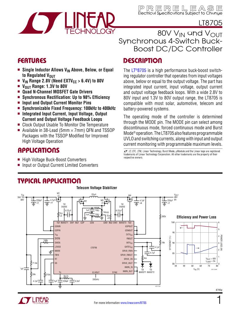
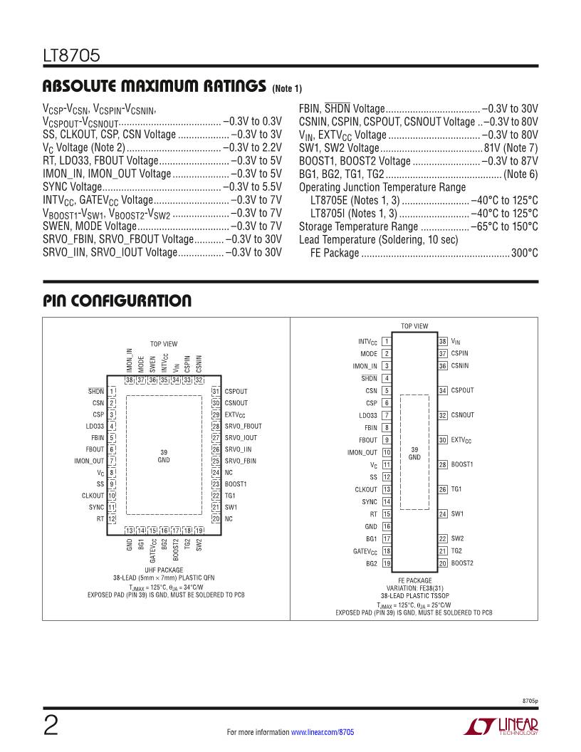
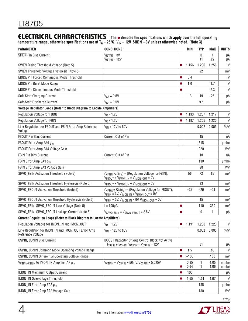
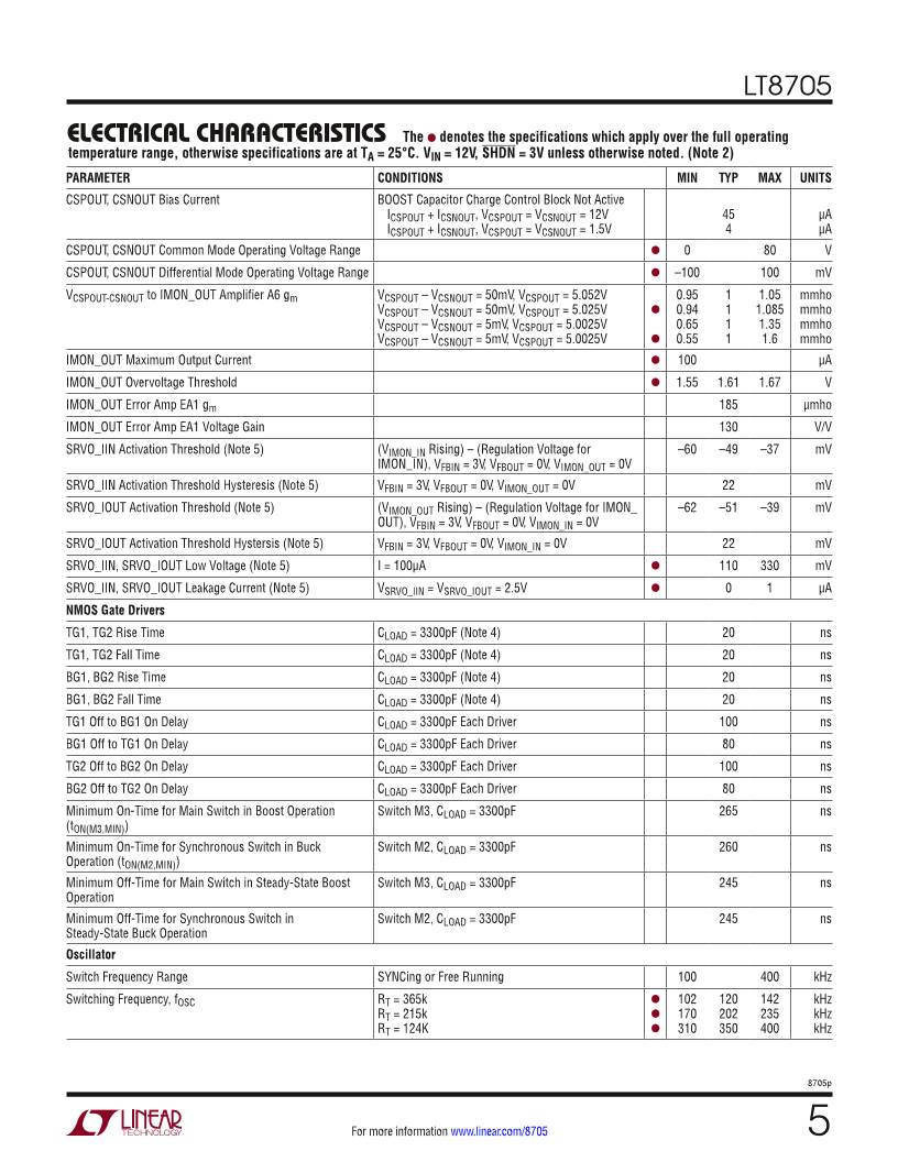
 WMS仓库系统