概要信息:
4-33
File Number 2284.2
CAUTION: These devices are sensitive to electrostatic discharge; follow proper ESD Handling Procedures.
http://www.intersil.com or 407-727-9207 | Copyright © Intersil Corporation 1999
IRF9640, RF1S9640SM
11A, 200V, 0.500 Ohm, P-Channel Power
MOSFETs
These are P-Channel enhancement mode silicon-gate
power field-effect transistors. They are advanced power
MOSFETs designed, tested, and guaranteed to withstand a
specified level of energy in the breakdown avalanche mode
of operation. All of these power MOSFETs are designed for
applications such as switching regulators, switching
converters, motor drivers, relay drivers and as drivers for
other high-power switching devices. The high input
impedance allows these types to be operated directly from
integrated circuits.
Formerly developmental type TA17522.
Features
• 11A, 200V
• rDS(ON) = 0.500Ω
• Single Pulse Avalanche Energy Rated
• SOA is Power Dissipation Limited
• Nanosecond Switching Speeds
• Linear Transfer Characteristics
• High Input Impedance
• Related Literature
- TB334, “Guidelines for Soldering Surface Mount
Components to PC Boards”
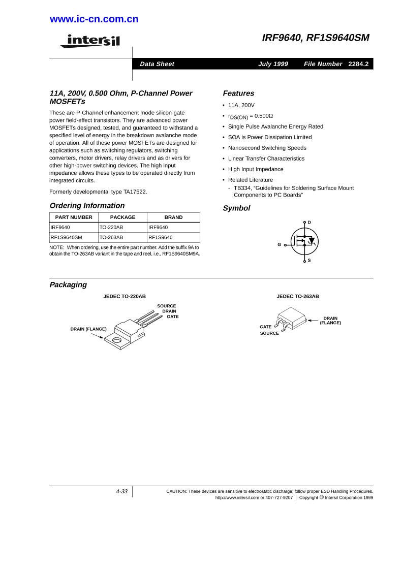
Symbol
Packaging
JEDEC TO-220AB JEDEC TO-263AB
Ordering Information
PART NUMBER PACKAGE BRAND
IRF9640 TO-220AB IRF9640
RF1S9640SM TO-263AB RF1S9640
NOTE: When ordering, use the entire part number. Add the suffix 9A to
obtain the TO-263AB variant in the tape and reel, i.e., RF1S9640SM9A.
G
D
S
GATE
DRAIN (FLANGE)
SOURCE
DRAIN
DRAIN
(FLANGE)
GATE
SOURCE
Data Sheet July 1999
www.ic-cn.com.cn
4-34
Absolute Maximum Ratings TC = 25oC, Unless Otherwise Specified
IRF9640, RF1S9640SM UNITS
Drain to Source Breakdown Voltage (Note 1) . . . . . . . . . . . . . . . . . . . . . . . . . . . . . . . . . . . . . . .VDS -200 V
Drain to Gate Voltage (RGS = 20kΩ) (Note 1) . . . . . . . . . . . . . . . . . . . . . . . . . . . . . . . . . . . . . VDGR -200 V
Continuous Drain Current . . . . . . . . . . . . . . . . . . . . . . . . . . . . . . . . . . . . . . . . . . . . . . . . . . . . . . . ID
TC = 100oC . . . . . . . . . . . . . . . . . . . . . . . . . . . . . . . . . . . . . . . . . . . . . . . . . . . . . . . . . . . . . . . . ID
-11
-7
A
A
Pulsed Drain Current (Note 2) . . . . . . . . . . . . . . . . . . . . . . . . . . . . . . . . . . . . . . . . . . . . . . . . . . . IDM -44 A
Gate to Source Voltage . . . . . . . . . . . . . . . . . . . . . . . . . . . . . . . . . . . . . . . . . . . . . . . . . . . . . . . .VGS ±20 V
Maximum Power Dissipation . . . . . . . . . . . . . . . . . . . . . . . . . . . . . . . . . . . . . . . . . . . . . . . . . . . . .PD 125 W
Linear Derating Factor . . . . . . . . . . . . . . . . . . . . . . . . . . . . . . . . . . . . . . . . . . . . . . . . . . . . . . . . . . 1 W/oC
Single Pulse Avalanche Energy Rating (Note 3, 4) . . . . . . . . . . . . . . . . . . . . . . . . . . . . . . . . . . . . .EAS 790 mJ
Operating and Storage Temperature . . . . . . . . . . . . . . . . . . . . . . . . . . . . . . . . . . . . . . . . . . TJ, TSTG -55 to 150 oC
Maximum Temperature for Soldering
Leads at 0.063in (1.6mm) from Case for 10s. . . . . . . . . . . . . . . . . . . . . . . . . . . . . . . . . . . . . . . TL
Package Body for 10s, See Techbrief 334 . . . . . . . . . . . . . . . . . . . . . . . . . . . . . . . . . . . . . . . Tpkg
300
260
oC
oC
CAUTION: Stresses above those listed in “Absolute Maximum Ratings” may cause permanent damage to the device. This is a stress only rating and operation of the
device at these or any other conditions above those indicated in the operational sections of this specification is not implied.
NOTE:
1. TJ = 25oC to 125oC
Electrical Specifications TC = 25oC, Unless Otherwise Specified
PARAMETER SYMBOL TEST CONDITIONS MIN TYP MAX UNITS
Drain to Source Breakdown Voltage BVDSS ID = -250µA, VGS = 0V (Figure 10) -200 - - V
Gate Threshold Voltage VGS(TH) VGS = VDS, ID = -250µA -2 - -4 V
Zero Gate Voltage Drain Current IDSS VDS = Rated BVDSS, VGS = 0V - - 25 µA
VDS = 0.8 x Rated BVDSS, VGS = 0V, TC = 125oC - - 250 µA
On-State Drain Current (Note 2) ID(ON) VDS > ID(ON) x rDS(ON)MAX, VGS = -10V -11 - - A
Gate to Source Leakage Current IGSS VGS = ±20V - - ±100 nA
Drain to Source On Resistance (Note 2) rDS(ON) ID = -6A, VGS = -10V (Figures 8, 9) - 0.350 0.500 Ω
Forward Transconductance (Note 2) gfs VDS > ID(ON) x rDS(ON)MAX, ID = -6A (Figure 12) 4 6 - S
Turn-On Delay Time td(ON) VDD = 0.5 x Rated BVDSS, ID ≈ -11A, RG = 9.1Ω
VGS = -10V (Figures 17, 18)
RL = 8.4Ω for VDSS = -100V
RL = 6.1Ω for VDSS = -75V
MOSFET Switching Times are Essentially Indepen-
dent of Operating Temperature
- 18 22 ns
Rise Time tr - 45 68 ns
Turn-Off Delay Time td(OFF) - 75 90 ns
Fall Time tf - 29 44 ns
Total Gate Charge
(Gate to Source + Gate to Drain)
Qg(TOT) VGS = -10V, ID = -11A, VDS = 0.8 x Rated BVDSS
Ig(REF) = -1.5mA (Figures 14, 19, 20)
Gate Charge is Essentially Independent of
Operating Temperature
- 70 90 nC
Gate to Source Charge Qgs - 55 - nC
Gate to Drain “Miller” Charge Qgd - 15 - nC
Input Capacitance CISS VDS = -25V, VGS = 0V, f = 1MHz
(Figure 11)
- 1100 - pF
Output Capacitance COSS - 375 - pF
Reverse Transfer Capacitance CRSS - 150 - pF
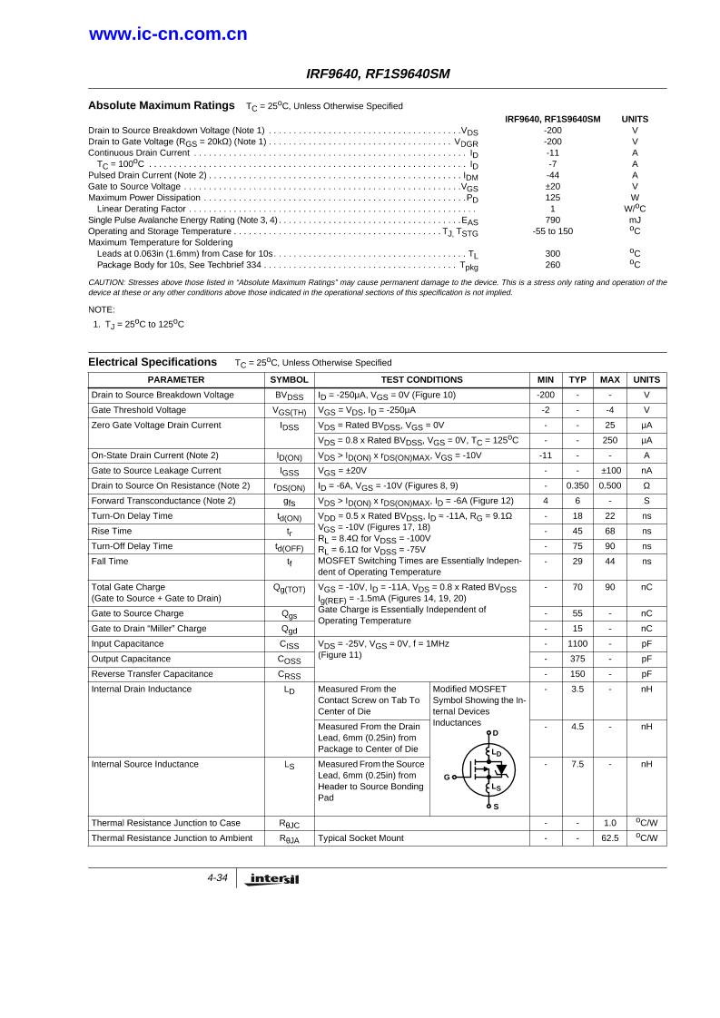
Internal Drain Inductance LD Measured From the
Contact Screw on Tab To
Center of Die
Modified MOSFET
Symbol Showing the In-
ternal Devices
Inductances
- 3.5 - nH
Measured From the Drain
Lead, 6mm (0.25in) from
Package to Center of Die
- 4.5 - nH
Internal Source Inductance LS Measured From the Source
Lead, 6mm (0.25in) from
Header to Source Bonding
Pad
- 7.5 - nH
Thermal Resistance Junction to Case RθJC - - 1.0 oC/W
Thermal Resistance Junction to Ambient RθJA Typical Socket Mount - - 62.5 oC/W
LS
LD
G
D
S
IRF9640, RF1S9640SM
www.ic-cn.com.cn
4-35
Source to Drain Diode Specifications
PARAMETER SYMBOL TEST CONDITIONS MIN TYP MAX UNITS
Continuous Source to Drain Current ISD Modified MOSFET Sym-
bol Showing the Integral
Reverse
P-N Junction Diode
- - -11 A
Pulse Source to Drain Current
(Note 3)
ISDM - - -44 A
Source to Drain Diode Voltage (Note 2) VSD TJ = 25oC, ISD = -11A, VGS = 0V (Figure 13) - - -1.5 V
Reverse Recovery Time trr TJ = 150oC, ISD = -11A, dISD/dt = 100A/µs - 300 - ns
Reverse Recovery Charge QRR TJ = 150oC, ISD = -11A, dISD/dt = 100A/µs - 1.9 - µC
NOTES:
2. Pulse Test: Pulse width ≤ 300µs, duty cycle ≤ 2%.
3. Repetitive Rating: Pulse width limited by Max junction temperature. See Transient Thermal Impedance curve (Figure 3).
4. VDD = 50V, starting TJ = 25oC, L = 9.8mH, RG = 25Ω, peak IAS = 11A. See Figures 15, 16.
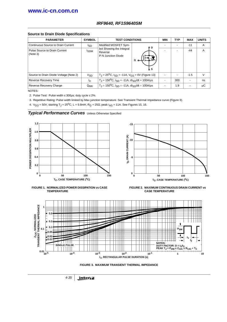
Typical Performance Curves Unless Otherwise Specified
FIGURE 1. NORMALIZED POWER DISSIPATION vs CASE
TEMPERATURE
FIGURE 2. MAXIMUM CONTINUOUS DRAIN CURRENT vs
CASE TEMPERATURE
FIGURE 3. MAXIMUM TRANSIENT THERMAL IMPEDANCE
G
D
S
0 50 100 150
0
TC, CASE TEMPERATURE (oC)
P
O
W
E
R
D
IS
S
IP
A
T
IO
N
M
U
LT
IP
L
IE
R
0.2
0.4
0.6
0.8
1.0
1.2
-5
0
0 50 100
I D
, D
R
A
IN
C
U
R
R
E
N
T
(
A
)
TC, CASE TEMPERATURE (oC)
-15
150
-10
t1, RECTANGULAR PULSE DURATION (s)
Z
θJ
C
, N
O
R
M
A
L
IZ
E
D
10-3 10-2
1
10-5 10-4
0.01
0.1
SINGLE PULSE
0.1
0.02
0.2
0.5
0.01
0.05
PDM
1010-1 1
NOTES:
DUTY FACTOR: D = t1/t2
PEAK TJ = PDM x ZθJC x RθJC + TC
t1
t2
T
R
A
N
S
IE
N
T
T
H
E
R
M
A
L
IM
P
E
D
A
N
C
E
IRF9640, RF1S9640SM
www.ic-cn.com.cn
4-36
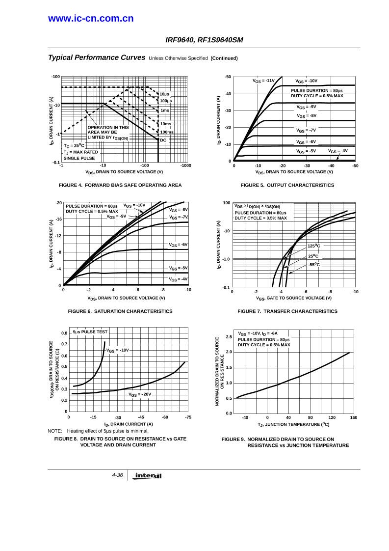
FIGURE 4. FORWARD BIAS SAFE OPERATING AREA FIGURE 5. OUTPUT CHARACTERISTICS
FIGURE 6. SATURATION CHARACTERISTICS FIGURE 7. TRANSFER CHARACTERISTICS
NOTE: Heating effect of 5µs pulse is minimal.
FIGURE 8. DRAIN TO SOURCE ON RESISTANCE vs GATE
VOLTAGE AND DRAIN CURRENT
FIGURE 9. NORMALIZED DRAIN TO SOURCE ON
RESISTANCE vs JUNCTION TEMPERATURE
Typical Performance Curves Unless Otherwise Specified (Continued)
VDS, DRAIN TO SOURCE VOLTAGE (V)
-10
I D
, D
R
A
IN
C
U
R
R
E
N
T
(
A
)
-100
-100
-1
100µs
10µs
DC
1ms
10ms
100ms
-10-1
LIMITED BY rDS(ON)
AREA MAY BE
OPERATION IN THIS
-0.1
-1000
TC = 25oC
SINGLE PULSE
TJ = MAX RATED
I D
, D
R
A
IN
C
U
R
R
E
N
T
(
A
)
0 -10 -20 -30 -40
-10
-20
-30
-40
-50
-50
VDS, DRAIN TO SOURCE VOLTAGE (V)
VGS = -11V VGS = -10V
VGS = -9V
VGS = -8V
VGS = -7V
VGS = -6V
VGS = -5V VGS = -4V
0
PULSE DURATION = 80µs
DUTY CYCLE = 0.5% MAX
-4
0 -2 -4 -6 -10
-8
-12
I D
, D
R
A
IN
C
U
R
R
E
N
T
(
A
)
VDS, DRAIN TO SOURCE VOLTAGE (V)
-16
-8
-20
VGS = -6V
VGS = -7V
VGS = -8V
VGS = -5V
VGS = -4V
VGS = -10V
VGS = -9V
PULSE DURATION = 80µs
DUTY CYCLE = 0.5% MAX
0
0 -4 -6 -8 -10-2
-0.1
-1.0
-10
I D
, D
R
A
IN
C
U
R
R
E
N
T
(
A
)
VGS, GATE TO SOURCE VOLTAGE (V)
100
125oC
25oC
-55oC
VDS ≥ I D(ON) x rDS(ON)
PULSE DURATION = 80µs
DUTY CYCLE = 0.5% MAX
0
0.3
0.6
0.7
-15 -30 -45 -60
r D
S
(O
N
),
D
R
A
IN
T
O
S
O
U
R
C
E
ID, DRAIN CURRENT (A)
-75
0.8
0
0.2
0.4
0.5
VGS = -10V
VGS = - 20V
5µs PULSE TEST
O
N
R
E
S
IS
TA
N
C
E
(
Ω
)
N
O
R
M
A
L
IZ
E
D
D
R
A
IN
T
O
S
O
U
R
C
E 2.5
1.5
1.0
0.5
0.0
-40 0 40
TJ, JUNCTION TEMPERATURE (oC)
120 160
2.0
80
VGS = -10V, ID = -6A
O
N
R
E
S
IS
TA
N
C
E
PULSE DURATION = 80µs
DUTY CYCLE = 0.5% MAX
IRF9640, RF1S9640SM
www.ic-cn.com.cn
4-37
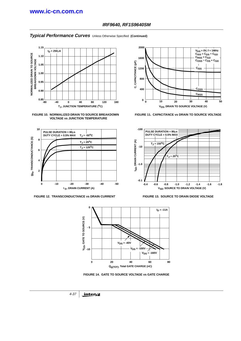
FIGURE 10. NORMALIZED DRAIN TO SOURCE BREAKDOWN
VOLTAGE vs JUNCTION TEMPERATURE
FIGURE 11. CAPACITANCE vs DRAIN TO SOURCE VOLTAGE
FIGURE 12. TRANSCONDUCTANCE vs DRAIN CURRENT FIGURE 13. SOURCE TO DRAIN DIODE VOLTAGE
FIGURE 14. GATE TO SOURCE VOLTAGE vs GATE CHARGE
Typical Performance Curves Unless Otherwise Specified (Continued)
1.15
1.00
0.95
0.90
0.85
-80 -40 0 40
TJ, JUNCTION TEMPERATURE (oC)
N
O
R
M
A
L
IZ
E
D
D
R
A
IN
T
O
S
O
U
R
C
E
B
R
E
A
K
D
O
W
N
V
O
LT
A
G
E
80 120 160
1.05
1.10
ID = 250µA
2000
400
0
0 20 50
C
, C
A
PA
C
IT
A
N
C
E
(
p
F
)
1200
VDS, DRAIN TO SOURCE VOLTAGE (V)
1600
800
CISS
COSS
CRSS
10 30 40
CISS = CGS + CGD
CRSS = CGD
COSS ≈ CDS + CGD
VGS = 0V, f = 1MHz
I D, DRAIN CURRENT (A)
g
fs
, T
R
A
N
S
C
O
N
D
U
C
TA
N
C
E
(
S
)
0 -10 -20 -30 -40
2
4
6
8
10
-50
TJ = 125oC
TJ = 25oC
TJ = -55oC
PULSE DURATION = 80µs
DUTY CYCLE = 0.5% MAX
-0.4 -1.0 -1.2 -1.6 -1.8-0.6
-0.1
-1.0
-10
I S
D
, D
R
A
IN
C
U
R
R
E
N
T
(
A
)
VSD, SOURCE TO DRAIN VOLTAGE (V)
-100
-0.8 -1.4
TJ = 25oC
TJ = 150oC
PULSE DURATION = 80µs
DUTY CYCLE = 0.5% MAX
Qg(TOT), Total GATE CHARGE (nC)
V
G
S
, G
A
T
E
T
O
S
O
U
R
C
E
(
V
)
0 20 40 60 80
-10
- 5
0
VDS = -40V
VDS = -100V
VDS = -160V
ID = -11A
IRF9640, RF1S9640SM
www.ic-cn.com.cn
4-38
Test Circuits and Waveforms
FIGURE 15. UNCLAMPED ENERGY TEST CIRCUIT FIGURE 16. UNCLAMPED ENERGY WAVEFORMS
FIGURE 17. SWITCHING TIME TEST CIRCUIT FIGURE 18. RESISTIVE SWITCHING WAVEFORMS
FIGURE 19. GATE CHARGE TEST CIRCUIT FIGURE 20. GATE CHARGE WAVEFORMS
tP
0.01Ω
L
IAS
+
-
VDS
VDD
RG
DUT
VARY tP TO OBTAIN
REQUIRED PEAK IAS
0V
VGS
VDD
VDS
BVDSS
tP
IAS
tAV
0
VGS
RL
RG
DUT
+
-
VDD
td(ON)
tr
90%
10%
VDS 90%
tf
td(OFF)
tOFF
90%
50%50%
10%
PULSE WIDTH
VGS
tON
10%
0
0
0.3µF
12V
BATTERY 50kΩ
+VDS
S
DUT
D
G
Ig(REF)
0
(ISOLATED
-VDS
0.2µF
CURRENT
REGULATOR
ID CURRENT
SAMPLING
IG CURRENT
SAMPLING
SUPPLY)
RESISTOR RESISTOR
DUT
Qg(TOT)
Qgd
Qgs
VDS
0
VGS
VDD
0
Ig(REF)
IRF9640, RF1S9640SM
www.ic-cn.com.cn
 WMS仓库系统