清华讲义《射频电路测试原理》-+第11讲+_+逻辑分析仪(LA).pdf
- 文件大小: 4.64MB
- 文件类型: pdf
- 上传日期: 2025-08-25
- 下载次数: 0
概要信息:
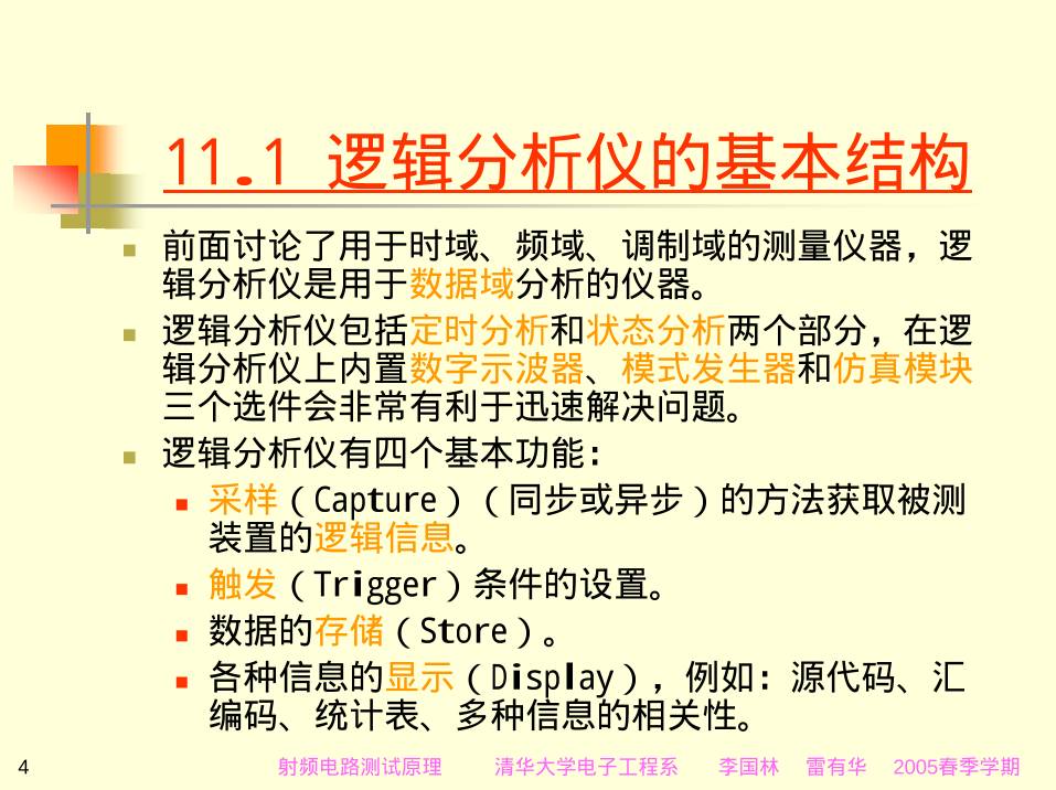
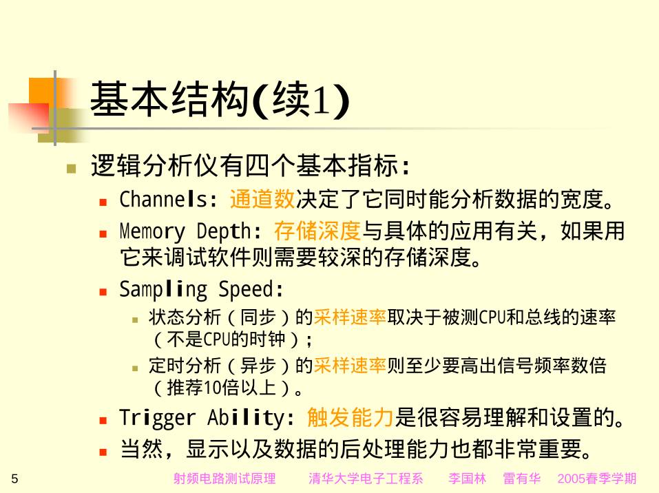
射频电路测试原理 第十一讲 逻辑分析仪(LA) leiyh@mail.tsinghua.edu.cn 射频电路测试原理 清华大学电子工程系 李国林 雷有华 2005春季学期2 参考文献 Agilent仪器说明书\16702B_逻辑分析系统\Service Guide_16700-97015.pdf ..\Help Volume_16700AB_5988-9058EN ..\Logic Analysis System Modules_5988-9439EN ..\16700 Catalog_5968-9661E ..\16702B Front Panel_B3760-92003 ..\Probing Solutions_5968-4632E ..\Installation Guide_16700-97023 ..\LAN 16702B help Volume ..\Training Kit_16700_97020 射频电路测试原理 清华大学电子工程系 李国林 雷有华 2005春季学期3 内容 11.1 逻辑分析仪的基本结构 11.2 逻辑分析仪的基本原理 11.3 定时分析和状态分析 11.4 模式发生器 11.5 16702B触发系统综述 11.6 进行基本测量 第五次实验 逻辑分析仪的使用 第十一讲 逻辑分析仪小结 射频电路测试原理 清华大学电子工程系 李国林 雷有华 2005春季学期4 11.1 逻辑分析仪的基本结构 前面讨论了用于时域、频域、调制域的测量仪器,逻 辑分析仪是用于数据域分析的仪器。 逻辑分析仪包括定时分析和状态分析两个部分,在逻 辑分析仪上内置数字示波器、模式发生器和仿真模块 三个选件会非常有利于迅速解决问题。 逻辑分析仪有四个基本功能: 采样(Capture)(同步或异步)的方法获取被测 装置的逻辑信息。 触发(Trigger)条件的设置。 数据的存储(Store)。 各种信息的显示(Display),例如:源代码、汇 编码、统计表、多种信息的相关性。 射频电路测试原理 清华大学电子工程系 李国林 雷有华 2005春季学期5 基本结构(续1) 逻辑分析仪有四个基本指标: Channels:通道数决定了它同时能分析数据的宽度。 Memory Depth:存储深度与具体的应用有关,如果用 它来调试软件则需要较深的存储深度。 Sampling Speed: 状态分析(同步)的采样速率取决于被测CPU和总线的速率 (不是CPU的时钟); 定时分析(异步)的采样速率则至少要高出信号频率数倍 (推荐10倍以上)。 Trigger Ability:触发能力是很容易理解和设置的。 当然,显示以及数据的后处理能力也都非常重要。 基本结构(续2) 本组现有的三种逻辑分析仪的主要指标如下表所示: 型号 E9340A 1673G 16702B 通道数 34 34 8160 状态速度 100MHz 135MHz 2Gsa/s 定时速度 250MHz 全通道250MHz 4Gsa/s 存储器深度 128K 64K 131M 探头 100K,8PF 100K,8PF 待讨论 触发 有12个序列级, 带10 个模式项; 2个跳变沿和毛刺项; 2个范围和定时器。 待讨论 16702B模块化逻辑分析系统 12吋LCD显示屏 触摸屏选择设置 专用菜单热键 显示位置热键 关触摸屏 标记热键 射频电路测试原理 清华大学电子工程系 李国林 雷有华 2005春季学期8 16702B前面 板与显示 Waveform Display. Listing Display. Mixed Display. Oscilloscape. 9 16702B后面板 10/100BaseT LAN并行打印端口 外接18GByte数据驱 动器或移动硬盘的 SCSI-II接口 40x CD-ROM 监视器接口 (选件 003) 可选用的仿真模块插槽或 多帧模块插槽 五 个 模 块 插 槽 (没有) 射频电路测试原理 清华大学电子工程系 李国林 雷有华 2005春季学期10 16702B主系统窗口 A.文件窗口 B.仪器图解 C.文件管理 D.运行 E.停止 F.系统显示 G.仪器配置显示 H.内部模块显示 I.运行状态显示 J.系统管理 K.处理器/总线设置 L.Demo M.仪器的状态显示 N.帮助 O.仪器背盖板显示 Target Control Port 射频电路测试原理 清华大学电子工程系 李国林 雷有华 2005春季学期11 16702B文件窗口 射频电路测试原理 清华大学电子工程系 李国林 雷有华 2005春季学期12 16702B逻辑分析系统特点 Windows窗口、触摸屏和模块化的设计; 硬件工程师利用逻辑分析系统可以揭示与软件 相关的硬件问题,例如中断管理等; 软件工程师可得到调试和分析工具,它克服了 传统仿真器的缺点,提供解决与硬件相关的软 件问题的相关方法; 系统工程师得到的时间相关显示可示出从所有 模拟信号到源代码的系统活动; 逻辑分析系统的交叉域显示能揭示硬件与软件 的交互问题,帮助设计师迅速而准确地从现象 跟踪到问题的产生原因。 1673G台式 逻辑分析仪 通道数 34; 状态速度 135MHz; 定时速度 全通道 250MHz; 存储器深度 64K; 触发: 有12个序列级, 带10个模式项; 2个跳变沿和毛刺 项; 2个范围和定时器。 射频电路测试原理 清华大学电子工程系 李国林 雷有华 2005春季学期14 E9340A PC 逻辑分析仪 通道数 34; 状态速度 100MHz; 定时速度 250MHz; 存储器深度 128K。 射频电路测试原理 清华大学电子工程系 李国林 雷有华 2005春季学期15 11.2 逻辑分析仪的基本原理 逻辑分析系统的基本原理如下图所示: 探头 采集 分析 通用探头 增强探头 分析探头 测量模块 仿真模块 16700/16600 逻辑分析 射频电路测试原理 清华大学电子工程系 李国林 雷有华 2005春季学期16 逻辑分析系统中的基本单元 射频电路测试原理 清华大学电子工程系 李国林 雷有华 2005春季学期17 方框原理图 CPU Board. PCI Board. Interface Board. Measurement Module Backplane. Emulation Module Interface. Power Supply. Expansion Frame. 射频电路测试原理 清华大学电子工程系 李国林 雷有华 2005春季学期18 11.2.1 探头 参考:\16702B_逻辑分析系统\Probing Solutions_5968-4632E.pdf 通用探头: 有40个引脚探头(用于16751A等模块); 和90个引脚探头(用于16753A等模块)。 射频电路测试原理 清华大学电子工程系 李国林 雷有华 2005春季学期19 Agilent探头 射频电路测试原理 清华大学电子工程系 李国林 雷有华 2005春季学期20 选择探头的基本原则 需要探测输入的信号个数; 探头附件易于连接到PC板上; 探头附件易于清洁; 信号的负载效应; 探头附件易于使用; 探头封装的类型; 封装探针之间的距离。 射频电路测试原理 清华大学电子工程系 李国林 雷有华 2005春季学期21 探头封装的类型 封装的类型有: DIP(Dual In-line Package); PGA(Pin Grid Array); BGA(Ball Grid Array); PLCC(Plastic Leaded Chip Carrier); PQFP(Plastic Quad Flat Pack); TQFP(Thin Quad Flat Pack); SOP(Small Outline Package); TSOP(Thin Small Outline Package)。 射频电路测试原理 清华大学电子工程系 李国林 雷有华 2005春季学期22 选择需要的探头 选择需要的探头: 是否需要分析微处理器? 是否需要特殊封装的探头? 中等密度探头的选择:01650-63203 adapter 和 01650-61608 17 channels; 高密度探头的选择:例如 E5385A等。 射频电路测试原理 清华大学电子工程系 李国林 雷有华 2005春季学期23 16751A测量模块的探头 The Agilent 01650-63203 isolation adapter The Agilent 01650-61608 17 channels 射频电路测试原理 清华大学电子工程系 李国林 雷有华 2005春季学期24 01650-61608有16个数据通道和1个时钟通道。 Sixteen-channel probe lead set 射频电路测试原理 清华大学电子工程系 李国林 雷有华 2005春季学期25 Probe housing and RC network housing 01650-61608的无源探头类似于示波器的无源 探头; 射频电路测试原理 清华大学电子工程系 李国林 雷有华 2005春季学期26 16720A模式发生器模块的探头 10460A TTL CLOCK POD; 10461A TTL DATA POD; 10477A 3.3V CLOCK POD; 10483A 3-STATE 3.3V DATA POD; 10498A 8-CH PROBE LEAD SET 6” 。 射频电路测试原理 清华大学电子工程系 李国林 雷有华 2005春季学期27 11.2.2 测量模块和仿真模块 根据需要来选择测量和仿真模块: 状态和定时模块:16751A(包括:Probing、 Comparators、Acquisition、Threshold 和 Test and clock synchronization circuit); 模式发生器模块:16720A(包括:Loop Register、 RAM、Output Driver、Clock Circuit、CPU Interface and Pod); 数字示波器模块(例如:16534A,本机没有); 仿真模块(本机没有)。 射频电路测试原理 清华大学电子工程系 李国林 雷有华 2005春季学期28 模块列表 射频电路测试原理 清华大学电子工程系 李国林 雷有华 2005春季学期29 现有数据分析模块 现有模块选件:A、B处没有,C、D处分别是: 16751A:Analyzer16M Sample 400MHz State/2GHz Timing Zoom(US40210797): 后面板对应的输出(在Pod Assignment的设置)为 C1、C2、C3和C4; 16751A:Analyzer 16M Sample 400MHz State/2GHz Timing Zoom(US40210796): 后面板对应的输出为D1、D2、D3和D4。 状态和定时模块16751A使用的是40个引脚的通 用逻辑分析探头(01650-61608)。 射频电路测试原理 清华大学电子工程系 李国林 雷有华 2005春季学期30 现有数据产生模块 现有模块选件E处是: 16720A:PattGen 300Mvector/s Pattern Generator(US39380609)。 模式发生器模块16720A可使用的接口夹有: 数据接口夹(10461ATTL数据接口夹、10483A 3态 TTL/3.3V数据接口夹) 时钟接口夹(10460A TTL时钟接口夹、 10477A 3.3V时钟接口夹)。 10498A 8-CH PROBE LEAD SET 6‘’。 11.2.3 数据显示 The most complete view of your system’s behavior. Viewing timing relationships between multiple buses and signals. Identify problem signals quickly by using eye scan to make eye diagram. View data patterns and sequences of events from the listing display. The captured binary data can be inverse assembled into processor mnemonics or displayed in multiple formats—binary, hex, decimal, octal, twos complement, ASCII or symbols. Correlate your logic analyzer trace to the high-level source code that produced it. 射频电路测试原理 清华大学电子工程系 李国林 雷有华 2005春季学期32 11.2.4 数据后处理分析 参考:\16702B_逻辑分析系统\16700 Catalog_5968-9661E.pdf 增加的数据后处理工具设置: 源相关性(B4620B P42); 数据通信(B4640B P47); 系统性能分析(B4600B P55); 串行分析(B4601B P62); 开发工具模块(B4605B P68)。 射频电路测试原理 清华大学电子工程系 李国林 雷有华 2005春季学期33 11.3 定时分析和状态分析 定时显示的逻辑分析仪与多踪示波器显示的波 形有某些相似之处。即它们都可以同时观测几 组波形; 但是逻辑分析仪只能用来测试逻辑电路,它显 示的波形与示波器显示的波形又有许多区别; 用定时显示的逻辑分析仪显示被分析的程序软 件很不直观,因此分析软件都用状态显示逻辑 分析仪; 无论定时显示或状态显示信号输入方式都是相 同的。 射频电路测试原理 清华大学电子工程系 李国林 雷有华 2005春季学期34 定时分析 首先,在Y方向上示波器是按比例显示输入信号的幅度, 但是逻辑分析仪的输入探头是个有源探头,它设置有 阈值电平,待测信号幅度超过阈值电平的部分显示为1 (对正逻辑为高电平),低于阈值电平的部分显示为0 (对正逻辑为低电平)。即逻辑分析仪在Y方向上只有 高、低电平的差别,而不显示输入信号幅度的比例关 系。 其次,示波器X方向上显示的时间是连续的。但是逻辑 分析仪则是以时钟为测量时间的单位,只有时钟到来 时,波形状态(高、低电平)才能转换为输入信号当 时所处的状态,两个时钟之间不能改变状态。即逻辑 分析仪的时间是量化的。 射频电路测试原理 清华大学电子工程系 李国林 雷有华 2005春季学期35 定时分析图解 射频电路测试原理 清华大学电子工程系 李国林 雷有华 2005春季学期36 状态分析 分析一段程序,必须将其中数据输入给状态分析仪, 也就是将CPU的地址线和数据线的逻辑状态输入给逻辑 分析仪; 逻辑分析仪可根据设置的各种要求,在每个时钟脉冲 到来时,采集一个数据字节。在采集若干个字节后, 在逻辑分析仪上按指定的格式显示。 必须恰当地选择时钟的频率,若时钟的频率过高,则 多次采集同一个数据;若时钟的频率过低,则会丢失 数据。 由于采集的数据存储在的存储器中,可长时间显示某 时刻的数据供分析用,这样就可发现偶然出错信息。 射频电路测试原理 清华大学电子工程系 李国林 雷有华 2005春季学期37 状态分析图解 射频电路测试原理 清华大学电子工程系 李国林 雷有华 2005春季学期38 定时和状态分析模块 Agilent的定时和状态分析模块特点: 存储器深度可达128M; 状态分析的采样速率可达1.5Gb/s; 定时分析窗口可达4GHz(250ps); VisiTrigger触发方式设置很有效。 射频电路测试原理 清华大学电子工程系 李国林 雷有华 2005春季学期 模块 窗口 设置 状态分析的时钟设置 信号线的颜色设置 访问状态分析选件 状态和定时选择 菜单选择 测量配置和 文件管理 LA采集数据 数据格式 触发方式设置 4GHz的定时分析窗口 射频电路测试原理 清华大学电子工程系 李国林 雷有华 2005春季学期40 11.4 模式发生器 为了配置能提供激励-响应测量的逻辑分析仪, 需要模式发生器。 软件工程师能在硬件电路完成之前,可利用模 块16720A产生罕见的测试条件并验证代码的工 作情况。 硬件工程师利用模块16720A能产生得到电路所 希望状态时需要的激励信号,可以全速运行电 路或步进运行通过电路的每一状态。 射频电路测试原理 清华大学电子工程系 李国林 雷有华 2005春季学期41 模式发生器模块16720A的特性 射频电路测试原理 清华大学电子工程系 李国林 雷有华 2005春季学期42 模式发生器模块的方框原理图 射频电路测试原理 清华大学电子工程系 李国林 雷有华 2005春季学期43 模式发生器模块的工作原理图 Loop Register:循环寄存器保存可编程的矢 量数据流; RAM:由五个256Kx16 VRAM和地址RAM组成, VRAM中存储所希望的模式数据; Output Driver:由一组锁存器/逻辑变换器和 多路器组成,锁存器/逻辑变换器将TTL电平信 号变换成输出的ECL电平信号,多路器将可编 程的数据送往输出通道; Clock Circuit:上述的三个电路共用; CPU Interface and Pod。 射频电路测试原理 清华大学电子工程系 李国林 雷有华 2005春季学期44 模式发生器模块的输出接口夹 模式发生器模块16720A可使用的接口夹有: 数据接口夹(10461ATTL数据接口夹、 10483A 3态TTL/3.3V数据接口夹) 时钟接口夹(10460A TTL时钟接口夹、 10477A 3.3V时钟接口夹)。 10498A 8-CH PROBE LEAD SET 6‘’。 射频电路测试原理 清华大学电子工程系 李国林 雷有华 2005春季学期45 11.5 16702B触发系统综述 利用图示的触发方式设置(VisiTrigger), 可以快速、方便地定位需要分析的问题。 16702B触发系统综述(本机总结): 定时分析共有27种触发形式(11.5.1到 11.5.27); 状态分析共有28种触发形式: 其中有12种触发形式与定时分析的触发形式相同 (11.5.10,11.5.17到 11.5.27); 与定时分析不同的触发形式共有16种(11.5.28到 11.5.43)。 VisiTrigger 触发数据标志设置模式和组合 触发沿设置 定时器设置 计数器设置 地址范围设置 触发序列 触发选择 当前状态信息 用户触发文本存取 射频电路测试原理 清华大学电子工程系 李国林 雷有华 2005春季学期47 11.5.1 Find pattern 模式触发: Occurrence 1 event Trigger Sequence 1 FIND PATTERN Find Label1 = XXXX Hex Then Trigger and fill memory 射频电路测试原理 清华大学电子工程系 李国林 雷有华 2005春季学期48 11.5.2 Find edge 波形的边沿触发: edge Trigger Sequence 1 FIND EDGE Find Label1 Edge Then Trigger and fill memory 11.5.3 Find edge AND pattern 波形的边沿和模式的“与”触发: pattern edge Trigger Sequence 1 FIND EDGE AND PATTERN Find Label1 Edge and Label1 = XXXX Hex Then Trigger and fill memory 11.5.4 Find width violation on pattern/pulse 模式或脉冲的宽度限定触发: Trigger Sequence 1 FIND WIDTH VIOLATION ON PATTERN/PULSE Find maximum or minimum width violation on Label1 = XXXX Hex min width 10 ns max width 15 ns Then Trigger and fill memory OR Max WidthMin Width Pulse too narrow Pulse too wide 11.5.5 Find Nth occurrence of an edge 第N次的波形边沿触发: …… edge edge Occurrence 1 Occurrence N Trigger Sequence 1 FIND NTH OCCURRENCE OF AN EDGE Find 1 occurrence of Label1 Edge Then Trigger and fill memory 11.5.6 Find pattern present for > duration 模式存在的时间宽度触发: pattern time Trigger Sequence 1 FIND PATTERN PRESENT FOR > DURATION Find Label1 = XXXX Hex Present for > 5 ns Then Trigger and fill memory 11.5.7 Find pattern present for < duration 模式存在的时间宽度触发: pattern time Trigger Sequence 1 FIND PATTERN PRESENT FOR < DURATION Find Label1 = XXXX Hex Present for < 10 ns Then Trigger and fill memory 11.5.8 Find pattern absent for > duration 模式不存在的时间宽度触发: NOT pattern time Trigger Sequence 1 FIND PATTERN ABSENT FOR > DURATION Find Label1 = XXXX Hex Present for > 5 ns Then Trigger and fill memory 射频电路测试原理 清华大学电子工程系 李国林 雷有华 2005春季学期55 11.5.9 Find pattern absent for < duration 模式不存在的时间宽度触发: NOT pattern time Trigger Sequence 1 FIND PATTERN ABSENT FOR < DURATION Find Label1 = XXXX Hex Present for < 10 ns Then Trigger and fill memory 射频电路测试原理 清华大学电子工程系 李国林 雷有华 2005春季学期56 11.5.10 Run until user stop 运行到用户定义停止: STOP。。。。。。。 Run Trigger Sequence 1 FIND UNTIL USER STOP 11.5.11 Find 2 edges too close together 两个波形边沿之间的宽度触发: edge 1 edge 2time Trigger Sequence 1 FIND 2 EDGES TOO CLOSE TOGETHER Find Label1 EDGE followed by Label1 EDGE Occurring within 15 ns Then Trigger and fill memory 11.5.12 Find 2 edges too far apart 两个波形边沿之间相隔的宽度触发: timeedge 1 edge 2 Trigger Sequence 1 FIND 2 EDGES TOO FAR APART Find a time period of 5 ns after Label1 Edge in which Label1 Edge does not occur Then Trigger and fill memory 11.5.13 Find pattern occurring too soon after edge 模式在波形边沿之后的触发: pattern time edge Trigger Sequence 1 FIND PATTERN OCCURRING TOO SOON AFTER EDGE Find Label1 = XXXX Hex occurring within 10 ns after Label1 Edge Then Trigger and fill memory 11.5.14 Find pattern occurring too late after edge 模式在波形边沿之之前的触发: pattern time edge Trigger Sequence 1 FIND PATTERN OCCURRING TOO LATE AFTER EDGE Find Label1 = XXXX Hex occurring within 10 ns after Label1 Edge Then Trigger and fill memory 射频电路测试原理 清华大学电子工程系 李国林 雷有华 2005春季学期61 11.5.15 Find glitch 毛刺触发: glitch Trigger Sequence 1 FIND GLITCH Find Label1 Edge * * * * * * * * * * * * * * * * Then Trigger and fill memory 射频电路测试原理 清华大学电子工程系 李国林 雷有华 2005春季学期62 11.5.16 Wait t seconds 等待时间 t 触发: tsec Run Trigger Trigger Sequence 1 WAIT T SECOND Wait 5 ns Then Trigger and fill memory 射频电路测试原理 清华大学电子工程系 李国林 雷有华 2005春季学期63 11.5.17 Wait for arm in 等待ARM输入触发: Wait for Arm IN The “Wait for arm in” functoon requires the nodule to be armed in the “Intermodule” menu, which can be accesssed through the “Navigate” butter, under “System”. 射频电路测试原理 清华大学电子工程系 李国林 雷有华 2005春季学期64 11.5.18 Wait for second analyzer to trigger 等待第二次分析时触发: Wait for 2nd analyzer The “Wait for other machine to trigger” functoon requires both machines to be turned on. The other machine can be activated through the “Navigate” butter, under “Activate Modules”. 射频电路测试原理 清华大学电子工程系 李国林 雷有华 2005春季学期65 11.5.19 Wait for flag 等待标记触发: 1 。。。。。。。 0 Trigger Sequence 1 WAIT FOR FLAG Wait for flag 1 Set Then Trigger and fill memory 射频电路测试原理 清华大学电子工程系 李国林 雷有华 2005春季学期66 11.5.20 Set/clear/pulse flag 置位、清除、脉冲时触发: SET1 CLEAR0 1 PULSE0 Trigger Sequence 1 SET/CLEAR/PULSE FLAG Flag 1 Set Then Trigger and fill memory 射频电路测试原理 清华大学电子工程系 李国林 雷有华 2005春季学期67 11.5.21 OR Trigger ARM 和 LABEL “或” 之后的触发: TRIGGER = ARM OR LABEL Possible causes: 1)This trigger function requires an Arm In from the “Intermodule” menu. 2)This trigger function requires at least one label. Make sure there is at least one label with bits assigned to it in the “Format” tab. 射频电路测试原理 清华大学电子工程系 李国林 雷有华 2005春季学期68 11.5.22 Advanced–If/then IF then IF--- THEN的触发: Trigger Sequence 1 If Label1 = XXXX Hex occurs 1 time Then Trigger and fill memory 射频电路测试原理 清华大学电子工程系 李国林 雷有华 2005春季学期69 11.5.23 Advanced–2-way branch IF then IF--- THEN或 ELSE的触发: else Trigger Sequence 1 If Label1 = XXXX Hex occurs 1 time Then Goto Next Else if Label1 = XXXX Hex Then Goto 1 11.5.24 Advanced 3-way branch IF--- THEN或 ELSE或 ELSE的触发: IF then Trigger Sequence 1 If Label1 = XXXX Hex occurs 1 time Then Goto Next Else if Label1 = XXXX Hex Then Goto 1 Else if Label1 = XXXX Hex Then Goto 1 else else 11.5.25 Advanced 4-way branch IF--- THEN或 ELSE或 ELSE或 ELSE的触发: IF Trigger Sequence 1 If Label1 = XXXX Hex occurs 1 time Then Goto Next Else if Label1 = XXXX Hex Then Goto 1 Else if Label1 = XXXX Hex Then Goto 1 Else if Label1 = XXXX Hex Then Goto 1 then elseelse else 11.5.26 Advanced – pattern1 AND pattern2 模式1和模式2的“与”触发: Pattern 1 AND Pattern 2Trigger Sequence 1 If Label1 = XXXX Hex AND Label1 = XXXX Hex occurs 1 time Then Trigger and fill memory 射频电路测试原理 清华大学电子工程系 李国林 雷有华 2005春季学期73 11.5.27 Advanced – pattern1 OR pattern2 模式1和模式2的“或”触发: Pattern 1 Pattern 2OR Trigger Sequence 1 If Label1 = XXXX Hex OR Label1 = XXXX Hex occurs 1 time Then Trigger and fill memory 射频电路测试原理 清华大学电子工程系 李国林 雷有华 2005春季学期74 11.5.28 Find pattern n times 产生第n次模式时触发: Pattern Pattern Occurrence 1 Occurrence n 。。。 Trigger Sequence 1 FIND PATTERN N TIMES Find 1 occurrence of Label1 = XXXX Hex Then Trigger and fill memory 11.5.29 Store range until pattern occurs 存储一个范围直到模式1产生才触发: Not pattern 1 Pattern 1 Pattern 1 does NOT occur here 。。。 Trigger Sequence 1 STORE RANGE UNTIL PATTERN OCCURS Store Label1 In range 0000 0000 Hex until Label1 = XXXX Hex occurs 1 time Then Store sample Goto Next Store range here 11.5.30 Store pattern2 until pattern1 occurs 存储模式2直到模式1产生才触发: Not pattern 1 Pattern 1 Pattern 1 does NOT occur here 。。。 Store pattern 2 here Trigger Sequence 1 STORE PATTERN2 UNTIL PATTERN1 OCCURS Store Label1 = XXXX Hex until Label1 = XXXX Hex occurs 1 time Then Store sample Goto Next 射频电路测试原理 清华大学电子工程系 李国林 雷有华 2005春季学期77 11.5.31 While storing pattern2, find pattern1 This function has been replaced。 For equivalent functionality, select either: Store pattern2 until pattern1 occurs or Store range until pattern occurs 11.5.32 Store nothing until pattern occurs 没有存储直到模式产生才触发: Not pattern Pattern Pattern does NOT occur here 。。。 Trigger Sequence 1 STORE NOTHING UNTIL PATTERN OCCURS Store nothing until Label1 = XXXX Hex Then Trigger and fill memory Store nothing here 射频电路测试原理 清华大学电子工程系 李国林 雷有华 2005春季学期79 11.5.33 Find pattern2 occurring immediately after pattern1 模式2在模式1之后立即产生才触发: Pattern 2Pattern 1 Trigger Sequence 1 STORE PATTERN2 OCCURRING IMMEDIATELY AFTER PATTERN1 Find Label1 = XXXX Hex immediately after Label1 = XXXX Hex Then Trigger and fill memory 射频电路测试原理 清华大学电子工程系 李国林 雷有华 2005春季学期80 11.5.34 Find pattern1 eventually followed by pattern2 模式1的后面紧跟模式2就触发: Pattern 2。。。Pattern 1 Trigger Sequence 1 FIND PATTERN1 EVENTUALLY FOLLOWED BY PATTERN1 Find Label1 = XXXX Hex eventually followed by Label1 = XXXX Hex Then Trigger and fill memory 11.5.35 Find pattern2 occurring too soon after pattern1 在模式1之后立即有模式2就触发: Pattern 1 Trigger Sequence 1 FIND PATTERN2 OCCCURRING TOO SOON AFTER PATTERN1 Find Label1 = XXXX Hex less then 100 ns after Label1 = XXXX Hex Use Time 1 Then Trigger and fill memory Pattern 2 time 11.5.36 Find pattern2 occurring too late after pattern1 在模式1之后足够远有模式2就触发: Pattern 1 Pattern 2Trigger Sequence 1 FIND PATTERN2 CCCURRING TOO LATE AFTER PATTERN1 Find a time period of 100 ns after Label1 = XXXX Hex in which Label1 = XXXX Hex doe not occur Use timer 1 Then Trigger and fill memory time 射频电路测试原理 清华大学电子工程系 李国林 雷有华 2005春季学期83 11.5.37 Find too few states between pattern1 and pattern2 模式1和模式2之间只有几个状态: Pattern 1 Pattern 2。。。 Less then n states occur here Trigger Sequence 1 FIND TOO FEW STATES BETWEEN PATTERN1 AND PATTERN2 Find Label1 = XXXX Hex after Label1 = XXXX Hex with less then 1 state occuring in between Then Trigger and fill memory 射频电路测试原理 清华大学电子工程系 李国林 雷有华 2005春季学期84 11.5.38 Find too many states between pattern1 and pattern2 模式1和模式2之间有许多个状态: Pattern 1 Pattern 2。。。 More then n states occur here Trigger Sequence 1 FIND TOO MANY STATES BETWEEN PATTERN1 ANDPATTERN2 Find 1 state after Label1 = XXXX Hex in which Label1 = XXXX Hex does not occur Then Trigger and fill memory 11.5.39 Find n-bit serial pattern 模式1和模式2之间有许多个状态: Serial pattern 1 0 1 0 1 0 1 0 1 0 1 0 1 0 time Trigger Sequence 1 FIND N-BIT SERIAL PATTERN Find 4 bit serial pattern 0000 LSB First on bit 0 of label Label1 Input base Binary Then Trigger and fill memory 11.5.40 Find pattern n consecutive times 模式连续地采样n次: 。。。Sample 1 Sample n pattern occurs here Trigger Sequence 1 FIND PATTERN1 N CONSECUTIVE TIMES Find 1 consecutive occurrence of Label1 = XXXX Hex Then Trigger and fill memory 11.5.41 Find pattern2 n times after pattern1 before pattern3 occurs 模式3出现前在模式1之后模式2出现n次: Pattern 1 Pattern 2。。。 Pattern 3 does NOT occur Pattern 2。。。 Occurrence 1 Occurrence n Trigger Sequence 1 FIND PATTERN2 N TIMES AFTER PATTERN1 BEFORE PATTERN3 OCCURS Find Label1 = XXXX Hex 1 time after Label1 = XXXX Hex before Label1 = XXXX Hex occurs Then Trigger and fill memory 射频电路测试原理 清华大学电子工程系 李国林 雷有华 2005春季学期88 11.5.42 Store n samples 模式连续地存储n次: 。。。Sample 1 Sample n Store here Trigger Sequence 1 STORE N SAMPLES Store 1 sample Then Trigger and fill memory 11.5.43 Wait n external clock states 等待第n个外时钟触发: Run Trigger Trigger Sequence 1 WAIT N EXTERNAL CLOCK STATES Wait 1 external clock state Then Trigger and fill memory 。。。 。。。 。。。。。。。。。 Clock 1 Clock 2 Clock n 90 11.6 进行基本测量 Hardware Turn-On:Hardware desigers verify its PCB basic operation brfore delivering it driver writers and software developers; Firmware Development:Given a PCB that has been turned-on,firmware developers create drivers and operating system; Software Development:Stable Hardware and driver software,software developers verify real-time application software execution; System Integration:When system problems are discovered,system integrators analyze system performance。 射频电路测试原理 清华大学电子工程系 李国林 雷有华 2005春季学期91 进行基本测量 参考:\16702B_逻辑分析系统\Training Kit_16700_97020.pdf Introduction to Timing Analysis: Trigger on an Edge Verify Pulse Widths Introduction to State Analysis: Trigger on an Event Trigger on a Sequence of Events Trigger on a 4 Bit Serial Pattern Trigger the Oscilloscope with the Timing Analyzer Using the Pattern Generator 射频电路测试原理 清华大学电子工程系 李国林 雷有华 2005春季学期92 Before You Begin 射频电路测试原理 清华大学电子工程系 李国林 雷有华 2005春季学期93 The Main System Window 射频电路测试原理 清华大学电子工程系 李国林 雷有华 2005春季学期94 The Measurement Process 射频电路测试原理 清华大学电子工程系 李国林 雷有华 2005春季学期95 11.6.1 Introduction to Timing Analysis: Trigger on an Edge 1.Select the analyzer you have connected to the credit card board. 2.Select Setup... from the pop-up menu to activate that instrument. 3.Select the Sampling tab. 4.Select Timing Mode. 射频电路测试原理 清华大学电子工程系 李国林 雷有华 2005春季学期96 Set Up the Bus Labels 1.Select the Format tab. 2.Select Label1, choose Rename. 3.Change the label name to TCOUNT. 4.To the far right of TCOUNT, select the field showing the 16 channels of pod 1. 5.Assign the lower 8 channels of pod 1 to TCOUNT by choosing “........********”. Define Trigger Conditions: Trigger on an Edge 1.Select the Trigger tab. 2.Under the Trigger Functions tab, select ‘Find edge’. 3.Select Replace to replace the default trigger sequence with the ‘Find edge’ trigger function. 4.Under Trigger Sequence 1, select. 5.Set Bit 7 as a rising edge and all other bits as don’t care. 6.Select OK. 射频电路测试原理 清华大学电子工程系 李国林 雷有华 2005春季学期98 Run the Analyzer and View the Data 1.Select the Run icon to capture the data. 2.Select the System icon. 3.Select the slot with the analyzer you are using, and choose Waveform from the pop-up menu. 4.To the right of the Seconds/div enter 20 ns. This will zoom in on the waveform. 射频电路测试原理 清华大学电子工程系 李国林 雷有华 2005春季学期99 Run the Analyzer and View the Data_1 Let’s expand the data so that you can look at all eight data lines. 5.Select TCOUNT all, and choose Expand. 射频电路测试原理 清华大学电子工程系 李国林 雷有华 2005春季学期100 Run the Analyzer and View the Data_2 Let’s change the color of data line TCOUNT 7 to red so that it stands out from the others. 6.Choose TCOUNT 7, and select Properties. 7.To the right of Color, select the red box, then choose OK. 射频电路测试原理 清华大学电子工程系 李国林 雷有华 2005春季学期101 11.6.2 Introduction to State Analysis: Trigger on an Event 射频电路测试原理 清华大学电子工程系 李国林 雷有华 2005春季学期102 Set Up the State Analyzer 1.Select the analyzer you have connected to the credit card board. 2.Select Setup... from the pop-up menu to activate that instrument. 3.Select the Sampling tab. 4.Select State Mode. 5.Select the under J, and choose Falling Edge. Set Up the Bus Labels 1.Select the Format tab. 2.Select Label1, choose Rename. 3.Change the label name to SCOUNT. 4.To the far right of SCOUNT, select the field showing the 16 channels of pod 1. 5.Assign the lower 8 channels of pod 1 to SCOUNT by choosing the “........********” selection in the pop-up menu. Define the Trigger Conditions: Trigger on an Event In this exercise, you will trigger on the pattern 3, and then only store the range 4-9 and pattern 10 until the analyzers memory is full. 1.Select the Trigger tab. 2.Under the Trigger Functions tab, select ‘Store nothing until pattern occurs’. 3.Select Replace to replace the default trigger sequence with the ‘Store nothing until pattern occurs’ trigger function. 4.In the Trigger Sequence box 1, choose Hex, then select Decimal from the pop-up menu. 5. Select the field to the right of SCOUNT =, and enter 003. 射频电路测试原理 清华大学电子工程系 李国林 雷有华 2005春季学期105 Define the Trigger Conditions: Trigger on an Event_1 6.Select Trigger and fill memory. 7.Select Trigger, then choose Trigger and goto. 射频电路测试原理 清华大学电子工程系 李国林 雷有华 2005春季学期106 Define the Trigger Conditions: Trigger on an Event_2 8.Under the Trigger Functions tab, select ‘Store range until pattern occurs’. 9.Select Insert after to insert the ‘Store range until patter occurs’ trigger function after Trigger Sequence 1. 10.In the Trigger Sequence 2, choose Hex, then select Decimal from the pop-up menu. Do this for both instances of Hex. 11.Select the first field to the right of Store SCOUNT In range, and enter 004. 12.Select the field to the right of 004 and enter 009. 13.Select the field to the right of until SCOUNT =, and enter 010. 射频电路测试原理 清华大学电子工程系 李国林 雷有华 2005春季学期107 Define the Trigger Conditions: Trigger on an Event_3 14.Select Next, then select 2. You may need to enlarge the window to see the Next button. 射频电路测试原理 清华大学电子工程系 李国林 雷有华 2005春季学期108 Run the Analyzer and View the Listing 1.Select the Run icon to capture the data. 2.Select the System icon. 3.Select the slot with the analyzer you are using, and select Listing.... 4.Under SCOUNT select Decimal. 射频电路测试原理 清华大学电子工程系 李国林 雷有华 2005春季学期109 Run the Analyzer and View the Listing_1 Because the credit card board counts from 0 to 255 repetitively, there are many occurrences of “4-9, 10.” Now you will search through the listing for the beginning of the stored range. 5.Select the field to the right of Decimal, enter 004. 6.Select the Next button to find the first occurrence of RANGE4-9. 7.Select the Next button a few more times. 射频电路测试原理 清华大学电子工程系 李国林 雷有华 2005春季学期110 11.6.3 Using the Pattern Generator Connect the Pattern Generator Connect the pattern generator output Pod 4 to the TTL Data Pod. Then connect the TTL Data Pod to J4 (labeled PATTERN GENERATOR) on the training board. 射频电路测试原理 清华大学电子工程系 李国林 雷有华 2005春季学期111 Connect the Pattern Generator 射频电路测试原理 清华大学电子工程系 李国林 雷有华 2005春季学期112 Set Up the Timing Analyzer 1.Select the analyzer you have connected to the credit card board. 2.Select Setup... from the pop-up menu to activate that instrument. 3.Select the Sampling tab. 4.Select Timing Mode. 射频电路测试原理 清华大学电子工程系 李国林 雷有华 2005春季学期113 Set Up the Bus Labels 1.Select the Format tab. 2.Select Label1, choose Rename. 3.Change the label name to PATGEN. 4.To the far right of PATGEN, select the field showing the 16 channels of pod 1. 5.Select Individual... from the pop-up menu. 6.Select channels eleven through eight. 7.Select OK. 射频电路测试原理 清华大学电子工程系 李国林 雷有华 2005春季学期114 Define the Trigger Conditions: Trigger on a 1 1.Select the Trigger tab. 2.The trigger function FIND PATTERN should be listed under Trigger Sequence 1. If it is not, select ‘Find pattern’ under the Trigger Functions tab, and choose Replace. 3 Select the field to the left of Hex, and enter 1. 射频电路测试原理 清华大学电子工程系 李国林 雷有华 2005春季学期115 Set Up the Pattern Generator In the Main System window, select the Pattern Generator, and choose Setup... 射频电路测试原理 清华大学电子工程系 李国林 雷有华 2005春季学期116 Set Up the Pattern Generator_1 2.Select the Format tab. 3.Select Label1, then choose Rename. 4.Change the label name to PATGEN. PATGEN is short for pattern generator, and represents the pattern generator data captured by the timing analyzer. 5.Select the field showing the 8 channels of pod 4. 6.Select Individual... from the pop-up menu. 7.Select channels three through zero, then choose OK. 射频电路测试原理 清华大学电子工程系 李国林 雷有华 2005春季学期117 Set Up the Pattern Generator_2 8.Set all channels on all other pods, except pod 4, to “don’t cares” by selecting ‘................’ from the pop-up menus. 射频电路测试原理 清华大学电子工程系 李国林 雷有华 2005春季学期118 Program the Pattern Generator Output 1.Select the Sequence tab. 2.Under the label PATGEN, select Hex, then choose Binary from the pop-up menu. 3.On line 3, after MAIN START, enter ‘0001’ over ‘0000’. 4.On line 4, enter ‘0010’. 射频电路测试原理 清华大学电子工程系 李国林 雷有华 2005春季学期119 Program the Pattern Generator Output_1 5.Select line 4, then choose Insert After, and then Vector. 6.On line 5, enter ‘0100’. 射频电路测试原理 清华大学电子工程系 李国林 雷有华 2005春季学期120 Program the Pattern Generator Output_2 7.Select line 5, then choose Insert After, and then Vector. Program the Pattern Generator Output_3 8.Select line 6, enter ‘1000’. Building a User Macro. A User Macro is a vector sequence defined by a custom name. Macros may be inserted into the INIT or MAIN sequences of the vectors in Sequence, or into other macros. 射频电路测试原理 清华大学电子工程系 李国林 雷有华 2005春季学期122 Start the Pattern Generator and View the Walking Ones Pattern 1.In the Pattern Generator window, select the Run Repetitive icon, to begin the repetitive run. 2.Select the Setup window of the analyzer you are using. 3.Select the Run icon. The Timing analyzer runs a single trace and automatically displays the Waveform 1 menu in which you see the "walking ones" pattern. 4.Select the System icon. 5.Select the slot with the analyzer you are using, and choose Waveform. 射频电路测试原理 清华大学电子工程系 李国林 雷有华 2005春季学期123 Start the Pattern Generator and View the Walking Ones Pattern Let’s expand the data so that you can look at all eight data lines. 6.Select PATGEN all, and select Expand. 7.To the right of the Seconds/div field enter 20 ns. This will zoom in on the waveform. 射频电路测试原理 清华大学电子工程系 李国林 雷有华 2005春季学期124 第五次实验 逻辑分析仪的使用 参考:\16702B_逻辑分析系统\Training Kit_16700_97020.pdf 利用 Credit Card Board E2433-66502 进行基本测量。 第十一讲 逻辑分析仪小结 逻辑分析仪的五个选件、四个基本功能和四个 基本指标 定时分析、状态分析、数字示波器、模式发生器和 仿真模块; 采样、触发、存储和显示; 通道数、存储深度、采样速率和触发能力; 定时分析和状态分析; 模式发生器; 16702B的触发系统; 利用 Credit Card Board E2433-66502进行基 本测量; 目前已有16900系列逻辑分析系统。 射频电路测试原理 清华大学电子工程系 李国林 雷有华 2005春季学期126 数字示波器模块 Bandwidth:dc to 500 MHz; Input R:1 Meg Ohm; 50 Ohms。 射频电路测试原理 清华大学电子工程系 李国林 雷有华 2005春季学期127 Agilent仿真探头 Setting Up an E5900A、E5900B Emulation Probe; Setting Up an E5901A、E5901B Emulation Module。 射频电路测试原理 清华大学电子工程系 李国林 雷有华 2005春季学期128 10460A TTL CLOCK POD 参考:\16702B_逻辑分析系统\16700 Catalog_5968-9661E.pdf 射频电路测试原理 清华大学电子工程系 李国林 雷有华 2005春季学期129 10461A TTL DATA POD 参考:\16702B_逻辑分析系统\16700 Catalog_5968-9661E.pdf 射频电路测试原理 清华大学电子工程系 李国林 雷有华 2005春季学期130 10477A 3.3V CLOCK POD 参考:\16702B_逻辑分析系统\16700 Catalog_5968- 9661E.pdf 射频电路测试原理 清华大学电子工程系 李国林 雷有华 2005春季学期131 10483A 3-STATE 3.3V DATA POD 参考:\16702B_逻辑分析系统\16700 Catalog_5968- 9661E.pdf 射频电路测试原理 清华大学电子工程系 李国林 雷有华 2005春季学期132 10498A 8-CH PROBE LEAD SET 6” Recommended lead set:10477A 3.3V CLOCK POD 和 10483A 3-STATE 3.3V DATA POD。 射频电路测试原理 清华大学电子工程系 李国林 雷有华 2005春季学期133 Target Control Port 参考:Help Volume_16700AB_5988- 9058EN.pdf The Target Control Port is an 8-bit, TTL port that you can use to send signals to your target system. It does not function like a pattern generator, but more like a remote control for the target's switches. 射频电路测试原理 清华大学电子工程系 李国林 雷有华 2005春季学期134 Target Control Port_1 The target control cable is keyed, so it can be inserted only one way.Plug it into the target control port with the key up and the cable hanging down. The lines are color-coded. Bit 0 is brown, bit 1 is red, bit 2 is orange,and so on up to bit 7 (grey). The black and white lines are both ground.Pins 0, 2, 4, and 6 are on the top of the connector and arranged in thesame order as the lines. If you plan on using Open Collector, remember to install pull-up resistors. The minimum pull- up resistor is 350 . and the maximum sink current into the Target Control Port is 12 mA. 射频电路测试原理 清华大学电子工程系 李国林 雷有华 2005春季学期135 Target Control Port_2 Resetting Your Target System 1. Attach the target control cable to the reset line, using proper termination. 2. Set up a label, RESET. 3. Set the value to 1, for high impedance. 4. Set Output Drive to Open Collector. 5. When the target needs to be reset manually, select Pulse. 射频电路测试原理 清华大学电子工程系 李国林 雷有华 2005春季学期136 多帧模块插槽 多帧模块插槽允许扩张连接高达8个16700B或 16702B多帧模块。 通道数高达8160个。 射频电路测试原理 清华大学电子工程系 李国林 雷有华 2005春季学期137 To connect a 16701B expander frame 16701B:Install your measurement modules in the 16701B expander frame。 射频电路测试原理 清华大学电子工程系 李国林 雷有华 2005春季学期138 Creating the Macro 1.In Macro, recall the macro that you want to create. 2.Select MACRO START. 3.Select Insert After, then select Vector. 4.Repeat for each new vector line you want to insert. 5.Select left-most character in the new vector line. 6.Enter in the desired vector data.. 7.Optional - Insert an instruction (see page 81) instead of entering vectordata. 8.Enter in a name for the new macro.. 9.Optional - Select Parameters and turn on any parameters you plan to use.
缩略图:

高速下载:
正在进行安全检测...
点击后进入安全下载页,再进行实际下载。下载链接有效期 24 小时,过期会自动刷新。
下载说明:
- 文件描述:清华讲义《射频电路测试原理》-+第11讲+_+逻辑分析仪(LA).pdf,可用于在线分享与下载使用。
- 文件分类:文档资料
- 用途建议:适用于资料分享、学习交流、办公协作。
- 适合人群:学生、教师、办公人员、项目协作团队。
- 适配系统:Windows、macOS、Android、iOS 均可下载访问。