02.混合信号测量.pdf
- 文件大小: 885.66KB
- 文件类型: pdf
- 上传日期: 2025-08-21
- 下载次数: 0
概要信息:
Basic Fundamental for Radio Frequency Circuits Testing
Lecture 2    Mixed Signal Test
ADC and DAC test
guolinli@tsinghua.edu.cn
射频电路测试原理 清华大学电子工程系 李国林 雷有华 2005春季学期2
Reference
Mark Baker, Demystifying Mixed-Signal Test Methods,
Elsevier Science, 2003
Mark Burns, Gordon W. Roberts, An Introduction to Mixed-
Signal IC Test and Measurement, Oxford University Press,
2001
Michael L. bushnell, Vishwani D. Agrawal, Essentials of
Electronic Testing for Digital, Memory and Mixed-Signal
VLSI Circuits, Kluwer Academic Publishers, London, 2002
陈光禹,王厚军,田书林,李为民,现代测试技术,电子科技大
学出版社,2002
董在望主编,通信电路原理,第二版,高等教育出版社,2002
射频电路测试原理 清华大学电子工程系 李国林 雷有华 2005春季学期3
Mark Baker, Demystifying Mixed-Signal Test Methods, Elsevier Science, 2003
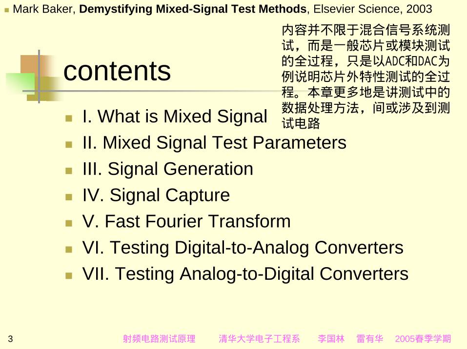
contents
I. What is Mixed Signal
II. Mixed Signal Test Parameters
III. Signal Generation
IV. Signal Capture
V. Fast Fourier Transform
VI. Testing Digital-to-Analog Converters
VII. Testing Analog-to-Digital Converters
内容并不限于混合信号系统测
试,而是一般芯片或模块测试
的全过程,只是以ADC和DAC为
例说明芯片外特性测试的全过
程。本章更多地是讲测试中的
数据处理方法,间或涉及到测
试电路
射频电路测试原理 清华大学电子工程系 李国林 雷有华 2005春季学期4
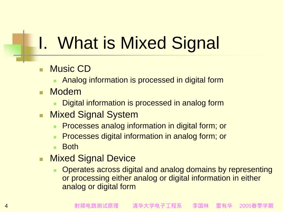
I.  What is Mixed Signal
Music CD
Analog information is processed in digital form
Modem
Digital information is processed in analog form
Mixed Signal System
Processes analog information in digital form; or
Processes digital information in analog form; or
Both
Mixed Signal Device
Operates across digital and analog domains by representing
or processing either analog or digital information in either
analog or digital form
射频电路测试原理 清华大学电子工程系 李国林 雷有华 2005春季学期5
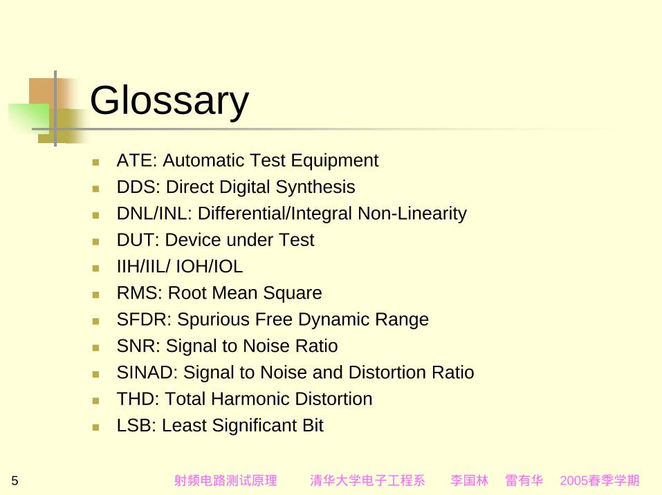
Glossary
ATE: Automatic Test Equipment
DDS: Direct Digital Synthesis
DNL/INL: Differential/Integral Non-Linearity
DUT: Device under Test
IIH/IIL/ IOH/IOL
RMS: Root Mean Square
SFDR: Spurious Free Dynamic Range
SNR: Signal to Noise Ratio
SINAD: Signal to Noise and Distortion Ratio
THD: Total Harmonic Distortion
LSB: Least Significant Bit
射频电路测试原理 清华大学电子工程系 李国林 雷有华 2005春季学期6
Mixed Signal Test System
Analog
Sequence
DAC
DUT
Capture
Data
ADC
DSP
Digital Pattern Compare Pass/
Fail
Pass/
Fail
Digital Logic
Digitized Analog
Timing
Driver Receiver
射频电路测试原理 清华大学电子工程系 李国林 雷有华 2005春季学期7
II. Mixed Signal Test Parameters
A large portion of mixed signal testing focuses on
signal analysis
The procedure for signal analysis is simple
Apply the condition
Make some measurements
And perform some calculations
What are you going to measure?
How can you determine if a mixed signal device is
operating according to specification?
We are looking for signal characteristic values, or the results
of the analysis, to be within a certain range
We’ll say it passes the test
射频电路测试原理 清华大学电子工程系 李国林 雷有华 2005春季学期8
Signal Analysis Categories
In general, signal analysis falls within one or more of
two distinct categories
DC, AC (Time Domain, and Frequency Domain)
DC: Direct Current signal analysis is used to
determine the static or quiescent characteristics of
the device
Such as supply current or output pin voltage levels
AC: Time Domain signal analysis applies to transient
or dynamic signal characteristics or frequency
domain signal analysis (FFT)
Typical time domain specifications include slew rate and
settling time
Typical frequency domain specifications include noise and
distortion
射频电路测试原理 清华大学电子工程系 李国林 雷有华 2005春季学期9
An Example:
Programmable Gain Amplifier
inA outA
OVR
GND
DDV EEV
0D1D2D
Analog Input
+12V -12V
Analog Output
Over-Limit Digital Output
(Logic high while output
level exceeds 10volts)
Gain Set Digital Input
射频电路测试原理 清华大学电子工程系 李国林 雷有华 2005春季学期10
Test Plan
The test engineer creates a test plan document
based on the device specification document or ‘spec
sheet’
The device specification document describes the operation
and electrical characteristics of the device
The order of tests is arranged in a sequence that will
most quickly identify possible defects
The most basic tests are usually performed first, with the
view that if the part fails the basic tests, then it is not
necessary to test it any further
For Example: Defect in the power supply pin connection
An output amplitude first test will give a result of functional failure.
射频电路测试原理 清华大学电子工程系 李国林 雷有华 2005春季学期11
Some Conventions
Firstly do some checking
Is the tester connected to the device?
Is the power supply current within spec?
IDD: If not, there’s no point in going further.
Is the input pin current within spec?
IIH/IIL: If the inputs do not work, nothing else will work.
If the connections, the power supply, and the inputs
are within specification, then make the Functional
Testing
Does the device perform the correct operational function?
Can the output pin generate the correct signal with the
specified current load?
Are the measured time domain and frequency domain
parameters within specification?
DC
AC
射频电路测试原理 清华大学电子工程系 李国林 雷有华 2005春季学期12
Example Device DC Specification
Analog Input Pins
Leakage = ±1uA@10V; Offset = ±2mV
Analog Output Pins
Maximum output voltage = ±10.5volts
Minimum positive output current = 5mA @+10volts
Minimum negative output current = -5mA @-10volts
Gain Error<2%
Linearity Error<1%
Digital Input Pins
IIL= ±1uA@0.0V; IIH = ±1uA@5.0V
VIL = 0.2V; VIH = 2.4V
Digital Output Pins
IOL = 5mA; IOH =-5mA; VOL = 0.2volts; VOH = 3.2volts
Threshold = 10volts/±0.1Volts
射频电路测试原理 清华大学电子工程系 李国林 雷有华 2005春季学期13
Creates a test plan based on the device spec sheet
Example Test List
Continuity: proper connection
Supply Current: Gross Process Error
Leakage Current
Offset Voltage: Function Verification
Maximum Analog Output
Over Level Function
Gain Error
Linearity Error: time consuming test
射频电路测试原理 清华大学电子工程系 李国林 雷有华 2005春季学期14
Continuity Test
The purpose of continuity tests is to verity that
the test system is properly connected to the
DUT
Verify that all DUT signal pins are connected to
the tester channels
Verify that the pins of the DUT are properly
connected to the internal device circuitry
Continuity tests do not check a specified
device parameter, and are not specified in the
data sheet
射频电路测试原理 清华大学电子工程系 李国林 雷有华 2005春季学期15
One method to detect pin-to-pin shorts is to perform the continuity test on each pin serially,
and to force all pins, except the pin under test, to 0.0 volts. If the pin under test is shorted
to another pin, the test will measure 0.0 volts instead of a diode drop voltage.
Testing the VDD Diode
DUT
Internal
Circuitry
VVDD 0=
VVEE 0=
PinDUT
Force 100uA
Measure diode drop
F
P
F
V8.0>
V5.0<
V7.0~6.0
The current force resource is typically set to clamp at 1.0 volt.
射频电路测试原理 清华大学电子工程系 李国林 雷有华 2005春季学期16
Supply Current Tests
The supply current tests verify that the DUT
supply current is not excessive
There are two methods for testing the device
supply current
Static testing: the device is not active
Dynamic testing: the device is active
The device runs the same sequence repeatedly until the
DC measurement is complete
The IDD current can be measured once the
device is in the specified condition
射频电路测试原理 清华大学电子工程系 李国林 雷有华 2005春季学期17
Power Supply Current Tests
Force all input pins to 0
volts (short)
Force all output pins to 0
mA (open)
Force VDD to +12.0volts
Force VEE to –12.0volts
Wait for the ATE
instruments and DUT to
settle
Measure IDD current and
compare with limits
Measure IEE current and
compare with limits
inA outA
OVR
GND
DDV
EEV
0D1D2D
+12V -12V
0A
0V
射频电路测试原理 清华大学电子工程系 李国林 雷有华 2005春季学期18
Input Pin Current Tests
Input pin current tests verify that the device inputs do
not require excessive drive current
Leakage tests
Leakage tests are performed with the power supply
pins set to the nominal operating level
IIL is tested by applying a logic state using the specified VIL
level, and measuring the current flow into the pin
IIH is tested by applying a logic state using the specified VIH
level, and measuring the current flow into the pin
To test pin-to-pin leakage, it is common practice to pre-set
the voltage level of all input pins to the opposite extreme of
the pin under test
射频电路测试原理 清华大学电子工程系 李国林 雷有华 2005春季学期19
Offset Voltage Tests
Offset voltage measures the voltage
correction required on the amplifier input to
force the amplifier output to zero volts
Because of process variation and imbalances in
the internal circuitry, a zero volt level on the
amplifier input does not always cause the amplifier
output to generate a zero voltage level
In that case, the input must be adjusted to achieve
a zero voltage output level.
The amount of required adjustment or correction is
the input offset.
射频电路测试原理 清华大学电子工程系 李国林 雷有华 2005春季学期20
Adjusting and Measuring Input
Level for Offset Test
DUTProgrammable
source
Measurement
System
DSP
To determine the input level that corresponds
to a known level on the output
射频电路测试原理 清华大学电子工程系 李国林 雷有华 2005春季学期21
In the end-use application, a device that cannot supply sufficient
current on the amplifier output pins will cause unreliable operation
Output Compliance Tests
Conductive parameter tests verify the drive capability
of the amplifier output pin by measuring the output
voltage level with a specified current load
Output current tests measure the current capacity on the
output pin of the device when the output level is at the
specified condition
Output voltage tests measure the voltage drive level on the
output pin of the device for a specified logic state
The output voltage drive level is tested by verifying that the
amplifier output can generate an acceptable voltage level
with a specified current load
射频电路测试原理 清华大学电子工程系 李国林 雷有华 2005春季学期22
Testing Output Voltage Compliance
Analog Output Pins
Maximum output voltage = ±10.5volts
Minimum positive output current = 5mA @+10volts
Minimum negative output current = -5mA @-10volts
The Current Output Low (IOL)
specification describes how
much current the output must
supply when generating a
negative voltage level
IOL: device sink current
Tester resource must source
current
The Current Output High (IOH)
specification describes how
much current the output must
supply when driving a logical
high
IOH: device source current
Tester resource must sink
current
inA outA
OVR
GND
DDV
EEV
0D1D2D
+12V -12V
Force 5mA
Measure
>=10.5V
10.5V
Should
goes to a
logic high0V
射频电路测试原理 清华大学电子工程系 李国林 雷有华 2005春季学期23
Over-Range Function
The device over-range function provides
an indication of an over-range condition
on the amplifier output via a logic level
on the OVR digital output pin
>10.1V: -5mA load: >3.2V
<9.9V: +5mA load: <0.2V
Digital Output Pins
IOL = 5mA; IOH = –5mA; VOL = 0.2volts; VOH = 3.2volts
Threshold = 10volts/±0.1Volts
射频电路测试原理 清华大学电子工程系 李国林 雷有华 2005春季学期24
Analog Output Pins
Gain Error<2%
Linearity Error<1%
Gain Error Tests
The gain test evaluates the overall span of
the amplifier output
voltsInputvoltawithSpanLevelOutputIdeal
VlOUTPUTLeveVINPUTLevelgGAINSettin
VlOUTPUTLeveVINPUTLevelgGAINSettin
Ideal
0.7  0.1
0.8     0.1     8
0.1     0.1     1
=
===
===
voltsInputvoltawithSpanLevelOutputActual
VlOUTPUTLeveVINPUTLevelgGAINSettin
VlOUTPUTLeveVINPUTLevelgGAINSettin
Actual
1.7  0.1
15.8     0.1     8
05.1     0.1     1
=
===
===
%42.1%100
0.7
0.71.7
=×
−
→
−
Ideal
IdealActual
射频电路测试原理 清华大学电子工程系 李国林 雷有华 2005春季学期25
Analog Output Pins
Gain Error<2%
Linearity Error<1%
Linearity Error Tests
Linearity error
measures each gain
step by changing the
gain setting with a
constant input
voltage level. The
incremental steps of
the output are
compared to a
calculated linear
‘straight line’.

Gain
Step
Calculated
Value
Measured
Value
Error
1 1.050 1.050 0.0%
2 2.064 2.107 +2.1%
3 3.078 3.301 -1.5%
4 4.092 4.051 -1.0%
5 5.106 5.116 +0.2%
6 6.120 6.193 +1.2%
7 7.134 7.060 -1.0%
8 8.150 8.150 0.0%

射频电路测试原理 清华大学电子工程系 李国林 雷有华 2005春季学期26
AC Tests
Time Domain Specifications
Slew Rate
10volts per us
Settling Time
5us
Frequency Response
100Hz to 10kHz ±4dB
Frequency Domain Specifications
Harmonic Distortion
<5% at 1000Hz at 1 volt
Signal to Noise
-60dB with 1000Hz reference at 1 volt
射频电路测试原理 清华大学电子工程系 李国林 雷有华 2005春季学期27
1
1.0
9.0
Slew Rate
Slew Rate describes the slope of a voltage
change across time
The DUT is driven with a fast edge pulse, and the
output is captured and analyzed
The slew rate is found as the slope of the
transition between the rated output extremes
Sometimes the positive and negative swing will
have different slew rates, in which case both
positive and negative slew rates are tested
射频电路测试原理 清华大学电子工程系 李国林 雷有华 2005春季学期28
Settling Time
Settling time measures the time elapsed from
the application of a step input to when the
amplifier output has settled to within a
specified error band of the final value
Settling time includes the time needed for the
DUT to slew from the initial value, recover
from any overload, and settle to within a
specified range
射频电路测试原理 清华大学电子工程系 李国林 雷有华 2005春季学期29
Slew Rate and Settling Time Test
inA outA
OVR
GND
DDV
EEV
0D1D2D
+12V -12V
Signal
Source
Signal
Capture
/Analyze
射频电路测试原理 清华大学电子工程系 李国林 雷有华 2005春季学期30
Time Domain Specifications
Frequency Response
100Hz to 10kHz ±4dB
Frequency Response Tests
A device may be specified to operated over a range
of signal frequencies. A frequency response test
measures how the device responds to different signal
frequencies across a specified range
applying a multi-tone signal, the device response to each
frequency component can be evaluated by processing the
device output in the frequency domain
The device is powered up and programmed for a
specific gain value
Using a set of different input signal frequency, measures the
output signal amplitude. Calculate the amplitude ratio of the
Max and the Min, it should be less than 4dB in a the
specified frequency range from 100Hz to 10kHz.
射频电路测试原理 清华大学电子工程系 李国林 雷有华 2005春季学期31
Distortion and Noise Testing
The test process for distortion and noise
testing applies a pure sine wave to the DUT.
The output of the DUT is captured and
processed with a Fourier Transform.
By evaluating the frequency domain data, the
amplitude of the original signal frequency can be
compared with the amplitude of the signal
distortion, which occurs at integer multiples of the
original frequency.
Signal information that is not the original signal
frequency and not an integer multiple of the
original frequency is identified as noise.
射频电路测试原理 清华大学电子工程系 李国林 雷有华 2005春季学期32
III. Signal Generation
Testing requires the ability to present a
stimulus, measure the response, and analyze
the results
The mechanism for presenting the stimulus is
referred to as source
The source instrumentation on a mixed signal
tester must be able to apply  analog data in
both analog form and digital form
DDS
source DUT capture analysis
射频电路测试原理 清华大学电子工程系 李国林 雷有华 2005春季学期33
Signal Source Hardware
Control
Source Data
Memory DAC Filter Amp
to DUT analog input
Control
Pattern
Memory Timing Format Driver
to DUT digital input
射频电路测试原理 清华大学电子工程系 李国林 雷有华 2005春季学期34
Digital Source Circuit Description
Digital Signal Source
A binary representation of the device functional pattern is
stored into test system signal source RAM. The digital signal
sequence is programmed as a series of vectors.
The digital signal source memory is accessed by the
sequence controller. The sequence controller looks up the
command and timing information for the selected vector and
applies the timing information to the formatter. Formatting
determines the edge placement timing within the vector
cycles of the data presented to the device input pins via the
pin driver. The pin driver acts as a high-speed switch that
converts the formatted data into voltage levels representing
the binary signal data.
射频电路测试原理 清华大学电子工程系 李国林 雷有华 2005春季学期35
Analog Source Circuit Description
Analog Signal Source
The clock is programmed to
the correct sample rate and
drives the sequencer and
the DAC
The sequencer steps
through addresses in the
source memory
The source memory
provides the sequence of
digital samples to the DAC
The DAC circuit converts
the digital samples into
analog levels
The reconstruction filter
smoothes the sequence of
discrete analog levels into a
continuous analog signal
The amplifier adjusts the
level of the signal required
by the DUT
Sequencer Clock
address
D
a
t
a
DAC Recon.
Filter Amp
Tester CPU
射频电路测试原理 清华大学电子工程系 李国林 雷有华 2005春季学期36
kHzfi 2= kHzfs 16= 32=samples 4=cycles Hzfbase 500=
DSP’s Law
Samples: sample size
Fs: sample frequency
Fi: frequency of interest
Fbase: base frequency
Cycles: number of signal cycles in the sample set
Hzf
cycles
samples
Hzf
kHzf
base
i
s
25
41
320
1025
8
=
=
=
=
=
samples
ff s
base =
base
i
f
fcycles =
cyclessamplesff is :: =
Fbase must have an integer relationship with both fs
and fi for that the samples and cycles must be
integers.
射频电路测试原理 清华大学电子工程系 李国林 雷有华 2005春季学期37
sinx/x
The number of samples per cycle directly affects the
quality of the generated signal
The process of representing a continuous wave
shape with a series of discrete steps introduces some
signal amplitude degenerations
The error of the ‘curve fit ’ is a function of the number of
samples per cycle,and can be predicted
si ffxx
xA π2
sin
==
9003.0sin
==
x
xA
kHzf
kHzf
i
s
1
8
=
= 7853.02 == si ffx π
射频电路测试原理 清华大学电子工程系 李国林 雷有华 2005春季学期38
Source Filter
The reconstruction filter of the analog source
hardware must be considered when choosing
the optimal number of samples per cycle
The purpose of the reconstruction filter is to
remove the effects of the sample clock,and the
DAC step rate
Typical reconstruction filters are designed to
attenuated the clock frequency by 24 dB for every
doubling of the pass band
A 24dB per octave reconstruction filer with a 1kHz pass
band will attenuate a 4kHz clock by only 48dB.
Inadequate number of samples per cycle will cause
distortion in output signal
射频电路测试原理 清华大学电子工程系 李国林 雷有华 2005春季学期39
IV. Signal Capture
A mixed signal device may generate analog
information in either analog or digital form, which in
turn is captured by the ATE systems’ signal capture
instruments
The contents of the signal capture memory represent
a digitized analog signal, not digital logic states
Instead of comparing the captured digitized signal with a
pattern, the signal data is analyzed by a digital signal
processor (DSP)
The DSP analyzes the signal data to extract analog signal
information, such as peak, RMS, signal-to-noise, and
harmonic distortion
射频电路测试原理 清华大学电子工程系 李国林 雷有华 2005春季学期40
Digital Signal Capture Hardware
Sequencer Timing set
information
Format,
Timing
Capture
Memory DSP
DUT
Digitized
Analog
Output
VOH
Logic
State
Decoder
Strobe
VOL
Logic Analyzer PC ProgramADC
射频电路测试原理 清华大学电子工程系 李国林 雷有华 2005春季学期41
Analog Signal Capture Hardware
Sequencer
Capture
Memory
address
data
ADC
Clock
LP filterAmp
AccuracyHighVerykHzµV
AccuracyHighMHzµV
SpeedHighMHzµV
  0011.020
 2.11516
 5024412
nApplicatioRate Conversion@1VResolutionBits
±
±
±
bitsMBkB 201~256 ∗
DSP
DUT
Analog
Output
Spectrum Analyzer
OscilloscopeDAC
射频电路测试原理 清华大学电子工程系 李国林 雷有华 2005春季学期42
The Digitizing Process
Digitizing an analog signal represents a continuous
signal with a series of discrete numeric values
To digitize means to sample and quantify
Not all data points on the continuous signal are captured
To represent a continuous signal with a series of discrete steps
The process of converting from analog to digital has
several inherent constraints
Quantizing Error/LSB/Digitizer Resolution
Sample Size and Sample Rate
射频电路测试原理 清华大学电子工程系 李国林 雷有华 2005春季学期43
Quantizing Error
VV
mVmV
mVmV
VV
µµ 38766553616
6.02.1409612
5.19391287
Error@5 QuantizingLSB@5Number CodeBits
When using a 16-bit capture instrument on a 5volt range, the
instrument returns a reading of 38uV. This may or may not
be the same as the actual signal level. Because of the
limitations of the digitizer, the actual level could be anywhere
from 0 volts to 76uV --- There is no way to tell without
improving the instrument resolution.
射频电路测试原理 清华大学电子工程系 李国林 雷有华 2005春季学期44
Sample Size and Sample Rate
The purpose of digitizing a signal is to construct a sample set
that represents the signal amplitude over time
The sample frequency is the rate at which the digitizer samples the
input signal for conversion to a set of discrete numeric values
Ideally, the greater the number of samples (i.e., the higher the
sample rate) that can be taken for any given signal duration, the
greater the accuracy of the digital representation
However, acquiring many samples may take longer than acquiring
fewer samples
Processing many samples usually takes longer than processing
fewer samples
The constraints of the digitizer limit the sample frequency
The practical rule is to digitize the signal with as few samples as
possible, but no fewer
射频电路测试原理 清华大学电子工程系 李国林 雷有华 2005春季学期45
Nyquist and ShannonO
( )fF
maxfmaxf− sf
f
Nyquist Sampling Limit
The sampling frequency must be greater
than twice the bandwidth of the signal
Shannon’s Theorem
IF a signal over a given period of time
contains no frequency components greater
than fx, then all of the needed information
can be captured with a sample rate of 2fx
射频电路测试原理 清华大学电子工程系 李国林 雷有华 2005春季学期46
Application Example
To calculate the actual minimum sample rate
requires understanding the actual signal
bandwidth, including distortion and noise
Test signal is 10kHz sine wave
Test for total harmonic distortion includes the 2nd
and 3rd harmonics
Test SNR ranging from 1kHz to 50kHz
The sample frequency must be greater than 100kHz ---
twice the bandwidth of interest
射频电路测试原理 清华大学电子工程系 李国林 雷有华 2005春季学期47
dB0
dB96−
1 2 4 8 16
The Anti-Alias Filter
Generally, the roll-off characteristic of the anti-alias filter
indicates that signal frequencies above the pass-band will be
rejected by 24dB for every doubling of the signal frequency
Suppose you selected a 1-kHz-band low-pass anti-alias filter
To accept all signal frequency below 1kHz, and to reject signal
frequencies above 1kHz
If the capture instrument sample rate (fs) is programmed to 16kHz,
then the Nyquist frequency would be 8kHz (fs/2)
8/1=23: the selected configuration of the anti-alias filter has an
attenuation of only –72dB at 8kHz
This would create inadequate filtering of spurious high-frequency signal
information, and could generate incorrect measurement results
In order to fully utilize the anti-alias filter, it is common practice to
choose a sample frequency that is at least 16 or 32 times the signal
bandwidth
射频电路测试原理 清华大学电子工程系 李国林 雷有华 2005春季学期48
Frequency Resolution
The value of the base frequency (fbase)
determines the step size in the
frequency domain
In the time domain, the value of fi/fbase
indicates the number of cycles in the
sample set
In the frequency domain, the value of
fi/fbase determines the signal location
fbase = frequency resolution
samples
f
cycles
ff si
base ==
射频电路测试原理 清华大学电子工程系 李国林 雷有华 2005春季学期49
Once of the constraints of the FFT is that the input data will be processed as if it were
periodic. The design of the FFT algorithm assumes that the data set can be duplicated
without introducing signal error.
Capture Periodic Sample Sets
Objective
Determine the duration of the sample window that will
capture an integer number of cycles for each frequency
component of the analog signal
Parameters
The duration of the sample window is determined by the
sample size and the sample rate
Process
Calculate the frequency resolution that divides evenly into all
of the frequency components of the analog signal
Once the fbase has been determined, you can derive the
proper sample size and sample rate
射频电路测试原理 清华大学电子工程系 李国林 雷有华 2005春季学期50
An Example
Our objective is to calculate the sample size
and sample rate for digitizing a multi-tone
signal composed of 1680Hz, 3750Hz, and
5460Hz
The largest common denominator
1680=2x2x2x2x3x5x7
3570=2x3x5x7x17
5460=2x2x3x5x7x13
Common factor=2x3x5x7=210
fbase=210Hz (/n)
Window duration=1/fabse=4.7619ms (*n)
26*2105460
17*2103570
8*2101680
=
=
=
射频电路测试原理 清华大学电子工程系 李国林 雷有华 2005春季学期51
Sample frequency
Once you capture a periodic sample set of the multi-
tone signal, you will perform a FFT to analyze the
data in the frequency domain
The FFT transform requires that the sample set be a
power of 2, so you need to choose the number of
samples and sample rate to produce an fbase of
210Hz and a power of 2 sample size
We also know that the sample frequency should be at
least 16 times the signal bandwidth, in order to make
the best use of the anti-alias filter
Hzff bands 8736016*546016* ==≥
射频电路测试原理 清华大学电子工程系 李国林 雷有华 2005春季学期52
( ) ( )n
nf
fsamples
base
s ×=≥= 416
 210
87360
Sample Size and Sample Frequency
We know the sample size must be greater than or equal to
416 samples to achieve the target capture parameters
To meet the FFT data set requirement, we must choose a
sample size that is a power of 2, and is also greater than 416
Hzsamplesff bases 107520512210 =∗=∗=
( )msn 762.4:1=92512 ==samples
1021024 ==samples
Hzsamplesff bases 1075201024115 =∗=∗=
( )msn 524.9:2=
172131072 ==samples
Hzsamplesff bases 1310721310721 =∗=∗=
( )sn 1:210=
射频电路测试原理 清华大学电子工程系 李国林 雷有华 2005春季学期53
Signal Averaging
Signal averaging is a method of canceling random
noise in the captured signal data set
By summing the signal data and then generating an
average, the random noise components are reduced
by a factor equal to the square root of the number of
averaged cycles
Because the signal information is periodic, the amplitude of
the averaged data is unity for the signal
Because the noise components are non-periodic, the
averaged data attenuates the nose information
射频电路测试原理 清华大学电子工程系 李国林 雷有华 2005春季学期54
samples
f
cycles
ff si
base ==
Capture Unique Data Points
In general, most mixed signal test application will return more
complete results if the captured data is not redundant
An non-integer ration of fs/fi allows each sample in the
captured data set to represent a unique point of the captured
signal
cycle.each for  points data 16 same ecollect th  will thissignal,  the toRelative
5 ,80 ,200 ,1 ,16 ===== cyclessamplesHzfkHzfkHzf baseis
kHzkHz
cycles
ff ss 2.192.11611 =×=⎟⎟
⎠
⎞
⎜⎜
⎝
⎛
+×← 962002.19 == HzkHzsamples
As a result, the capture duration, and therefore the signal
acquisition time, is the same even though more information is
being gathered
射频电路测试原理 清华大学电子工程系 李国林 雷有华 2005春季学期55
Over-Sampling
In applications where the sample per cycle ratio is small, the
digitizer can be programmed to capture unique points on the
signal for each cycle. By composting several cycles, the end
result is an effective sample rate, that is higher than the actual
fs
To capture a 200kHz signal at 10.0MHz sample rate. The
constraints of the ATE system capture instrumentation are such
that the maximum sample clock (fs) is 1MHz
ns
MHzf
T
desireds
samplingovers 100
10
11
,
, ===−
ns
MHzf
T
s
s 1000
1
11
max,
min, ===
kHzkHz
T
f
actuals
actuals 909...0909.9091
,
, ≈==
cyclessampleskHzkHzff is 200:909200:909: ==
nsTTT samplingoverssactuals 1100,min,, =+= −
射频电路测试原理 清华大学电子工程系 李国林 雷有华 2005春季学期56
V. Fast Fourier Transform
The Fourier transform is a math process that
converts data from the time domain to the
frequency domain
The Fast Fourier transform is an efficient computer
algorithm for executing the Fourier transform
process
The FFT is used to extract frequency domain
information for tests including SNR, harmonic
distortion, and frequency response
射频电路测试原理 清华大学电子工程系 李国林 雷有华 2005春季学期57
The Fourier series is used to calculate complex frequency spectrum data based on periodic time
domain data. The Fourier integral is used to obtain complex frequency spectrum data based on
non-recurring time domain data.
Fourier Series
Mixed signal testing focuses primarily on the Fourier
series rather than the Fourier integral, and the
analysis of periodic data
Dirichlet requirement: A finite number of minima and maxima;
a finite number of discontinuities; and integrable in any
period
In mixed signal test applications, we can use the
Fourier series as a extremely useful function that
accepts time domain data and produces frequency
domain data, or vice versa
Time domain
data
Fourier
Series
Frequency domain
data
射频电路测试原理 清华大学电子工程系 李国林 雷有华 2005春季学期58
The Fourier Series Equation
The Fourier series, or discrete Fourier
transform acts like a tunable band-pass filter
in increments of the base frequency
The DFT would be tuned to DC, then f0, then 2f0,
3f0, and so on
If there are any components in the data set that
correspond to DC (, f0, 2f0, 3f0, …), then the
function results in a non-zero product
If there is no component, the function product is zero
( ) ( )∑
∞
=
++=
1
000 2sin2cos
n
nn tfnbtfnaatx ππ
射频电路测试原理 清华大学电子工程系 李国林 雷有华 2005春季学期59
binfrequency
f
fcycles
base
i  ==
Fbase and Frequency Bin
The output of the FFT is complex in type. Most test
applications convert the complex data to magnitude
information. Once the data is in magnitude format,
the frequency domain data can be viewed as an
array of energy values ranging from 0Hz to fs/2
The action of the FFT is to sort the signal frequencies
into a sequential set of frequency bins
The cycles value is identical to the frequency domain
array element location for that frequency
Time domain: number of cycles in the data set
Frequency domain: the signal frequency bin location
射频电路测试原理 清华大学电子工程系 李国林 雷有华 2005春季学期60
Nyquist and Shannon
The sample rate must be greater than twice the
signal frequency
The sample set must have more than two samples
per cycle of the signal
The frequency domain data set is valid from DC to
one-half of the sample frequency
The number of data points in the frequency domain is
one-half the number of data points in the time domain
The number of frequency fbins is always one-half the time
domain sample size
In order to capture at least two samples per cycle, the
signal frequency can be no greater than one-half of
the sample frequency
射频电路测试原理 清华大学电子工程系 李国林 雷有华 2005春季学期61
%59.4
97.0
6.44
97.0
1542 22
==
+
=
V
mV
V
mVTHD
Harmonic Distortion Tests Using the FFT
A distorted 5kHz sine wave is captured at a
32kHz clock rate with 256 samples
HzkHz
samples
ff s
base 125
256
32
===
128
2
 ==
samplesBinsFrequencyNumber of
( )kHzftoDCa Set fromDomain DatFrequency s 16
2

V
Hz
kHz
f
fBinsFrequencyl signalFundamenta
base
i 97.0:40
125
5  ===
mV
f
fBinsFrequencysignalHarmonicSecond
base
i 42:802    ==
mV
f
fBinsFrequencysignalHarmonicThird
base
i 15:1203    ==
射频电路测试原理 清华大学电子工程系 李国林 雷有华 2005春季学期62
22
log20
HarmoicNoise
SignalSINAD
+
=
SNR Testing Using the FFT
Measure the signal amplitude
DC n1 n2 n3 n4 S n5 n6 n7 n8 2H n9
Null out the DC, signal, and harmonics
Extract the algebraic sum of the noise
components
n10n11n12 3H n13
0 n1 n2 n3 n4 0 n5 n6 n7 n8 0 n9 n10n11n12 0 n13
...2
2
2
1 ++= nnNoise
Noise
SignalSNR log20=
射频电路测试原理 清华大学电子工程系 李国林 雷有华 2005春季学期63
Brick Wall Filters
Processing signal data in the frequency domain
allows the signal to be digitally filtered. One of the
advantage of processing information in the frequency
domain in precise delineation between the signal
component and spurious components
A Brick wall filter gets its name from the extremely
sharp cut-off frequency. The digitized signal is
converted to frequency domain data by the FFT. The
output of the FFT is processed to remove all of the
energy components above the desired frequency limit.
After the unwanted energy has been removed, the
time domain signal can be reconstructed by means of
a reverse FFT
射频电路测试原理 清华大学电子工程系 李国林 雷有华 2005春季学期64
Mathematical Over-Sampling
In application where it is not possible to capture the signal with a
sufficient number of samples for each cycle, it is sometimes
useful to interpolated between sample points
To execute mathematical over-sampling, the digitized data is
converted to the frequency domain
Recall that the span of data in the output of a FFT is equal to one-
half of the sample frequency.
Increasing the sample frequency for a given window duration has
the effect of increasing the number of samples, and extending the
FFT data set span
The frequency domain data is processed by appending to the
frequency domain data set, which in effect extends the
bandwidth. The appended frequency domain data is then
processed with a reverse FFT
射频电路测试原理 清华大学电子工程系 李国林 雷有华 2005春季学期65
Minimizing Frequency Domain Anomalies
Anomalies in the time domain data set can result in
erroneous data in the frequency domain. Once
frequency domain errors are resent, it often is very
difficult to separate valid data from spurious
information. Some of the time domain characteristics
that can degrade the result of the FFT are
Non-periodic Sample Sets and Leakage
Aliasing
Settling Time
DC Offset
Noise
Small errors in the time domain cab
create large errors in the frequency
domain. However, by understanding
and anticipating possible sources of
error, frequency domain anomalies
can be minimized.
射频电路测试原理 清华大学电子工程系 李国林 雷有华 2005春季学期66
Time Domain Window
The process of generating a finite sample set in the
time domain generates data points that are
processed by the FFT
Without the time window data, the FFT would convert
the signal into a single line spectra
When the sample window contains a signal, the time
domain data of the signal and the window data are
rolled together by the action of the FFT (convolution)
The result of windowed data in the frequency domain is that
the data has the amplitude and the frequency location of the
signal, and the sinx/x shape of the window
射频电路测试原理 清华大学电子工程系 李国林 雷有华 2005春季学期67
Non-Periodic Signal
Fortunately, the FFT acts like a filter bank at fbase increments.
The sinx/x energy from the window convolution is always at zero
at fbase increments.
As long as our data stays on fbase boundaries, the effects of the
window energy convolution will not be a problem
However, signal data that is not periodic will result in frequency
domain energy that is not at multiples of the frequency
resolution (fbase). Signal energy that is not at fbase increments
is not filtered by the action of the FFT, and instead is summed
with the side-band energy from the window data.The signal data
leaks into adjacent frequency bins
The result of leakage error is that power is taken from frequency
components existing in the time domain signal and transferred to
frequency components that do not exist in the time domain signal
射频电路测试原理 清华大学电子工程系 李国林 雷有华 2005春季学期68
Solutions to frequency Leakage Error
Make sure the fbase ratio is an exact integer
sub-multiple of the signal frequency
If the introduction of spurious signal
information cannot be avoided, choose an
fbase ratio that can accommodate both the
signal and the spurious frequency
Keeping in mind that the frequency domain
resolution is an inverse function of test time, it
may not be practical to choose a sufficiently
small fbase. In that case, a technique known
as windowing may provide a solution
射频电路测试原理 清华大学电子工程系 李国林 雷有华 2005春季学期69
Windowing Time Domain Data
In applications where the time domain data con not easily be
captured as a periodic data set, it is often helpful to process the
time domain data to modify the signal amplitude
By minimizing the signal amplitude at the end-points of the
capture window, the spurious effects on non-periodic data are
minimized
However, the effects of the signal attenuation must be
accounted for when the modulated time domain data is
converted to frequency domain data
Some common window algorithms are Hanning, Hamming, and
Blackman
Window algorithms have the effect of reducing the effects of a
non-periodic sample set, at the cost of reduced information and
lower precision in the frequency domain
射频电路测试原理 清华大学电子工程系 李国林 雷有华 2005春季学期70
Signal Aliasing
Nyquist’s Theorem states that properly
representing a waveform requires a sample
rate of at least twice the signal frequency.
Another way of applying Nyquist’s theorem is
to state that only sampled frequencies that
occur below fs/2 can be properly processed.
What happens to signals that are above the
Nyquist frequency?
The effect of aliasing is that signal frequencies
above the Nyquist point (fs/2) are folded back to
appear as lower frequency signals
射频电路测试原理 清华大学电子工程系 李国林 雷有华 2005春季学期71
Signal Aliasing
1if1is ff − 2ifsi ff −2
2sf sf
射频电路测试原理 清华大学电子工程系 李国林 雷有华 2005春季学期72
Under-Sampling Techniques
In applications that have a signal frequency
component above the Nyquist limit of the
digitizer, the alias effect can be used to
effectively extend the digitizer range
Let’s say you’ve got a signal with a frequency of
1.2MHz, but your digitizer has a maximum clock
rate of 1.0MHz. Because 1.2MHz is 200kHz above
the sampling frequency, the signal alias will show
up at 200kHz with exactly the same amplitude of
the original 1.2MHz signal.
射频电路测试原理 清华大学电子工程系 李国林 雷有华 2005春季学期73
Under-Sampling Techniques
By carefully choosing a sample frequency,
the application can place the Nyquist point at
any value. As a result, the alias frequency of
the high-frequency component can be
precisely placed anywhere in the frequency
spectrum
The amplitude of the alias will be exactly the
same as the amplitude of the original signal.
Limited only by the bandwidth of the digitizer.
It is therefore the bandwidth, not the maximum
sample rate, that is the frequency limit of the
digitizer
射频电路测试原理 清华大学电子工程系 李国林 雷有华 2005春季学期74
VI. Testing Digital-to-Analog Converters
Testing the DC performance of a DAC
consists largely of verifying a
consistent and linear response
A typical test setup for testing the DC
performance of a DAC device uses the
test system signal source to generate a
ramp
Efficient analysis of the device
response requires that the output
voltage be digitized and then
processed by the test system’s DSP
The DSP is used to subtract the
digitized DAC output from a calculated
ideal
The difference between the ideal and
actual signal data is analyzed to
evaluate DC performance
Source Memory
DAC  (DUT)
ADC
Capture RAM
DSP
Spectrum Analyzer
Oscilloscope
射频电路测试原理 清华大学电子工程系 李国林 雷有华 2005春季学期75
Digitizer
In order to test the accuracy of each DAC
output voltage, the resolution of the test
system digitizer must be much grater than the
resolution of the DAC under test
For linearity testing, the rule of thumb for testing
DACs is that the test system digitizer must have a
resolution of at least 2 bits greater than the
resolution of the DAC.
DUT: 12bit DAC 10volt: step=10.0/4096=2.44mV
16bit digitizer: step 152.5uV: 6.25%
射频电路测试原理 清华大学电子工程系 李国林 雷有华 2005春季学期76
DAC Overview
In general, a DAC
is specified
according to the
number of bits (n),
and the reference
level, also known
as the full-scale
range (FSR)
The output of a
perfect unipolar
DAC is one LSB
step less than the
reference voltage
0
8
1
8
28
3 8
4
8
5 8
68
7
1
001 010 011 100 101 110 111000
射频电路测试原理 清华大学电子工程系 李国林 雷有华 2005春季学期77
DC Test Overview
There are two general categories of DC tests
for DAC devices.
The first category evaluates the device minimum
and maximum output levels, referenced to an
absolute specification
Offset measures the minimum output level, while gain
measures the overall output span from the minimum to
the maximum
The second category of DC test evaluates the
device linearity, according to a relative step size
value that is calculated per device
射频电路测试原理 清华大学电子工程系 李国林 雷有华 2005春季学期78
Offset Measurement
DAC offset is the difference between the ideal and
actual analog output for a ‘zero code’ digital input
Some devices have a correction circuit to adjust offset
voltage, but offset may be tested as a worst-case
measurement without the correction circuit active
Testing for offset consist of measuring the analog
output generated by ‘zero code’ digital input and
comparing the value against acceptable limits
Offset may be specified as a voltage, a fraction of an
ideal LSB step, or a percentage of the ideal reference
level or FSR
射频电路测试原理 清华大学电子工程系 李国林 雷有华 2005春季学期79
LLL
Measure
VVDD 0.12+=VVREF 0.5+=
Offset Test
Apply power to the
device power pins
Apply the voltage
reference level to the
VREF pin
Set the VIL and VIH
level for digital input
pins
Apply the digital input
code corresponding to
zero voltage output
Measure the analog
output level and
evaluate the results
ideal
actual
offset
000
射频电路测试原理 清华大学电子工程系 李国林 雷有华 2005春季学期80
Gain Measurement
Gain is the difference between the ideal and
actual span of analog output values
corresponding to the full range of digital input
codes
To measure the output span, the test process
must measure both the minimum output level (at
‘all zeros’), and the maximum output level (at ‘all
ones’)
The difference between the minimum and
maximum output levels is specified as the
device gain
射频电路测试原理 清华大学电子工程系 李国林 雷有华 2005春季学期81
Gain Test
[ ] [ ] %1001
2
12
012 ×
⎟
⎟
⎟
⎟
⎠
⎞
⎜
⎜
⎜
⎜
⎝
⎛
−
−
×
−−
=
n
n
n
Ref Level
VVErrorGain
HHH
Measure
VVDD 0.12+=VVREF 0.5+=
Apply power to the device
power pins
Apply the voltage reference
level to the VREF pin
Set the VIL and VIH level for
digital input pins
Apply the digital input code
corresponding to the
maximum voltage output
Measure the analog output
level
Subtract the measured offset
value from the measured
maximum output level
Calculate the gain error and
evaluate against test limits
ideal actual
000
SpanIdeal
SpanMeasuredGain


=
111 input
digital
input
analog
offset
射频电路测试原理 清华大学电子工程系 李国林 雷有华 2005春季学期82
[ ] [ ]
12
012
−
−−
= n
n VVDeviceLSB
Linearity Test Overview
Ideally, each step of the DAC digital input value
would increment the DAC analog output by exactly
one step
In an actual device, the analog step size varies
Differential Nonlinearity (DNL) is the difference
between the actual step size and the calculated step
size
Integral Nonlinearity (INL) is the worst-case variation
in any of the analog output values with respect to an
ideal straight line drawn through the endpoints
INL is a way of measuring the accumulated linearity over the
entire range
射频电路测试原理 清华大学电子工程系 李国林 雷有华 2005春季学期83
Linearity Tests
Apply power to the device power
pins
Apply the voltage reference level
to the VREF pin
Set the VIL and VIH level for
digital input pins
Apply a ramp sequence of digital
input code
Measure and record the analog
output level for each code
Calculate the DNL and INL from
the analog output values
RAMP
Measure
VVDD 0.12+=VVREF 0.5+=
射频电路测试原理 清华大学电子工程系 李国林 雷有华 2005春季学期84
[ ] [ ] [ ] 11
−
−−
=
DeviceLSB
iViViDNL
DNL Tests Example
4bit FSR=10volts (0-9.375volts)
0000: 0.01volts; 1111: 9.985volts
DeviceLSB=(9.985-0.01)/15=0.665volts
…
1100: 8.00volts; 1101: 8.70volts
DNL[13]=(8.70-8.00)/0.665-1=
0.05DeviceLSB
射频电路测试原理 清华大学电子工程系 李国林 雷有华 2005春季学期85
[ ] [ ] [ ]( )
DeviceLSB
DeviceLSBiViViINL ×+−
=
0
INL Tests Example
0111: 4.98volts
Expected: 0.01+7×0.665=4.675volts
INL[7]=(4.98-4.675)/0.665
=0.46DeviceLSB
[ ] [ ]∑
=
=
i
j
iDNLiINL
1
[ ] [ ] [ ]1−−= iINLiINLiDNL
射频电路测试原理 清华大学电子工程系 李国林 雷有华 2005春季学期86
Missing Steps
A DAC has a missing step if an increase in
the digital code input does not result in an
increase in the analog output.
Testing for missing steps consists of checking
that every increase in the digital input code
causes a corresponding increase in the
analog output level
No missing steps can be inferred by testing for
DNL errors of less than ½LSB value
射频电路测试原理 清华大学电子工程系 李国林 雷有华 2005春季学期87
Monotonicity
A DAC is said to be monotonic if the transfer
characteristic slope has the same sign over the entire
range
A DAC is non-monotonic if an increase in the digital code
input causes a decrease in the analog output value
Testing that a DAC is monotonic consists of checking
that every increase in the digital input code causes a
corresponding analog output level that is greater than,
or equal to, the analog level from the previous code
Monotonic performance can be inferred by testing for DNL
errors of less than 1 LSB value
射频电路测试原理 清华大学电子工程系 李国林 雷有华 2005春季学期88
AC Test Overview
Testing the AC performance of a DAC
requires applying an AC signal or step
function, capturing the DAC device output,
and evaluating the response
As it turns out, not all DACs require the same type
of AC testing. In fact, some device types do not
require any AC testing at all because the end-use
application is essentially static
Even for devices that do require AC testing, not all
AC parameters make sense
The significant AC parameters are defined by the
application
射频电路测试原理 清华大学电子工程系 李国林 雷有华 2005春季学期89
Source Memory DAC  (DUT) ADC Capture RAM DSP
Digitizer
The test program must digitize the device output signal and then
process the signal data with the test system’s DSP.
In the case of DC testing, the system requirements concern
amplitude resolution
In the case of AC testing, the speed of the digitizer is of greater
concern than in DC testing
Some test systems have a choice of digitizers, allowing the test
engineer to choose between a high-accuracy digitizer for DC
tests, and a high-speed digitizer for AC tests
The theoretical minimum digitizer frequency is derived from
Nyquist’s theorem, which states that the digitizing sample rate must
be at least twice the frequency of the input signal. In practice, it is
more common to use a sample rate that is 8 or 16 times greater
than the signal frequency, in order to provide the proper frequency
resolution.
射频电路测试原理 清华大学电子工程系 李国林 雷有华 2005春季学期90
Some AC Specification
Slew Rate
The slope of the analog output signal across amplitude and time
Settling Time
The elapsed time between the beginning of the analog output
signal transition and the new analog output level
Glitch Impulse Area (振铃面积)
The amount of analog output amplitude variations across time
Distortion
The ratio of periodic signal error amplitude to signal amplitude
Signal-to-Noise Ratio
The ratio of non-periodic error amplitude to signal amplitude
射频电路测试原理 清华大学电子工程系 李国林 雷有华 2005春季学期91
Test System Requirement
AC, or dynamic, testing of DAC requires time domain
and frequency domain measurements. The test
system must be capable of
Synchronizing the digital input codes with the device under
test
Measuring the time delay between the digital input and the
analog output
Producing a sequence of digital codes that represent a
dynamic analog signal
Capturing the dynamic analog signal produced by the device
Performance time domain and frequency domain
measurements or analysis on the captured dynamic analog
signal
射频电路测试原理 清华大学电子工程系 李国林 雷有华 2005春季学期92
Slew Rate Test
To test slew rate, the DAC is driven with a step
function digital input sequence, such as the
minimum input code followed by the maximum
input code
In response, the analog output of the DAC should swing
from the minimum to the maximum value.
The captured signal from the device output is
analyzed by the DSP unit
The DSP calculates the slew rate by measuring the
period between two thresholds of the signal slope
射频电路测试原理 清华大学电子工程系 李国林 雷有华 2005春季学期93
Slew Rate Test Sequence
Apply power to the device
power pins
Apply the voltage
reference level to the
VREF pin
Set the VIL and VIH level
for the digital input pins
Apply a step function
sequence of digital input
codes
Capture the analog output
response
Use a DSP sequence to
evaluate the time between
the beginning of the slope
transition to the upper
slope threshold
射频电路测试原理 清华大学电子工程系 李国林 雷有华 2005春季学期94
Settling Time Test
Settling time of a DAC is usually defined as
the time from beginning of the analog output
transition until the DAC analog output settles
to within a certain tolerance, typically ½ of an
LSB
Settling time therefore expresses the device
‘propagation delay’ in terms of analog
performance
Evaluating settling time measures the transition
from a ±1/2 LSB band centered around the initial
value, until the output settles within ±1/2 LSB of
the final value
射频电路测试原理 清华大学电子工程系 李国林 雷有华 2005春季学期95
Settling Time Test Sequence
Apply power to the device
power pins
Apply the voltage
reference level to the
VREF pin
Set the VIL and VIH level
for the digital input pins
Apply a step function
sequence of digital input
codes
Capture the analog output
response
Use a DSP sequence to
evaluate the time between
the initial analog output
transition and the settled
analog output value
000
111
射频电路测试原理 清华大学电子工程系 李国林 雷有华 2005春季学期96
Glitch Impulse Area Test
0111
1000
pico-volts times seconds
Spurious transitions in a DAC analog output level are referred to
as ‘glitches’
Glitch testing is often performed at the transitions where all of
the digital input bits are changing state---for example, at mid
scale
0111 at just below mid-scale
1000 at mid scale
The output level should change by a single LSB for this example code
transition.
However, internal to the device, all of the switches must change
state. Timing skews and switch delays cause temporary glitches
to occur in the analog output before reaching the new level
Because the practical effects of glitching depend on both duration
and amplitude of the spurious output, both the duration and
amplitude of the glitch are measured together as ‘glitch area’
Glitch-less DACs: Sigma Delta DAC//SHA
射频电路测试原理 清华大学电子工程系 李国林 雷有华 2005春季学期97
Source Memory DAC  (DUT) ADC Capture RAM DSP
Dynamic Performance Tests
The overall effects of nonlinearity (DNL and
INL) together with glitch impulses across the
entire range of digital codes is sometimes
more easily expressed in terms of the DAC’s
ability to accurately produce a full-scale
analog signal
Testing for AC signal integrity requires that
the device be driven with a digital sine wave,
which is synchronized with the DAC
conversion rate to make sure a maximum
number of codes are tested
射频电路测试原理 清华大学电子工程系 李国林 雷有华 2005春季学期98
Sine Wave Histogram
Consider a histogram of s single cycle sine
wave
At the positive and negative peaks, the slope is
not as steep as the slope at zero crossing
Grouping the sine wave data set according to the
number of events per value will show a large
number of events around the peak values, and a
small number of events at zero crossing
In order to generate samples at all possible
codes, the input data set is designed to
generate at least five cycles of the signal
frequency
射频电路测试原理 清华大学电子工程系 李国林 雷有华 2005春季学期99
Harmonic Distortion Test
The DSP system is used to perform a fast
Fourier transform to convert the captured
data into frequency domain information
The frequency domain data generated by the FFT
is analyzed by first measuring the amplitude of
input signal frequency, which becomes the
reference point for the harmonic content ratio
The amplitudes for the frequencies that are integer
multiples of the signal frequency are measured
and summed, and then the results are calculated
as a percentage, or as a dB ratio
射频电路测试原理 清华大学电子工程系 李国林 雷有华 2005春季学期100
Example
The DUT is programmed to generate 5 cycles
of a 750-Hz sine wave. The data is captured
at 19.2kHz, with a total of 128 samples
HzkHz
samples
ff s
base 150
128
2.19
===
5
150
750__ ===
base
i
f
fbinfrequencylfundamenta
,...15,10__ =binfrequencyharmonic
mVHHHDistortion 6.6432 222 =++=
dB
mV
mV
lFundamenta
DistortionTHD 47.43
985
6.6log20log20 −===
射频电路测试原理 清华大学电子工程系 李国林 雷有华 2005春季学期101
Signal-to-Noise Tests
The same frequency domain data set that is used to
determine harmonic distortion can also be processed
to derive the signal-to-noise ratio.
By convention, the classic signal-to-noise measurement
does not include the harmonic energy, only the non-
harmonic error components
Testing for the SNR processes the result of the FFT to
remove the energy components due to the DC value, the
signal energy, and the harmonic energy
Because the SNR test is a statistical measurement, a
valid number of noise components must be
processed in order to generate a valid result.
The capture rate (fs) and sample size must be chosen to
produce a statistically valid number of data points, and a
suitable bandwidth corresponding to the SNR specification
射频电路测试原理 清华大学电子工程系 李国林 雷有华 2005春季学期102
VII. Testing Analog-to-Digital Converters
Much of the terminology for ADC testing is
similar to the terminology for DAC testing, but
the methodology is much different
An analog-to-digital converter is non-
deterministic from the output to the input. If a
test condition specifies a certain voltage on
the input of a perfect ADC, one can predict
the digital output code. However, if only the
digital output code is known, there is no way
to predict the exact input voltage --- only its
range can be predicted.
射频电路测试原理 清华大学电子工程系 李国林 雷有华 2005春季学期103
Test Setup
Like a DAC, testing the DC performance of an
ADC consists largely of verifying a consistent
and linear response
A typical test setup for testing the DC
performance of an ADC device uses the test
system signal source to generate an input
voltage ramp via the ATE signal generator
Whereas DAC testing requires a high-precision
measurement system to verify the analog output,
ADC testing requires a high-precision signal
generator to produce high-accuracy analog input
levels
射频电路测试原理 清华大学电子工程系 李国林 雷有华 2005春季学期104
ADC Test Overview
ADC (DUT)
Capture RAM
Source DAC Source Memory
DSP
High resolution
PC Program
Logic Analyzer
Programmable Clock
射频电路测试原理 清华大学电子工程系 李国林 雷有华 2005春季学期105
ADC Overview
An analog-to-digital converter will generate a single
output code for a range on input levels
The all-zero code does not have a corresponding input
range, only an upper threshold.
Likewise, the maximum output code identifies the threshold
transition point, but there is not a corresponding range of
values that correlates to the maximum output code
The next higher code is output when the input level
exceeds a given threshold
Evaluating the linearity of an ADC device measures the
voltage range between code thresholds
射频电路测试原理 清华大学电子工程系 李国林 雷有华 2005春季学期106
ADC Transfer Curve
Linearity tests for an
ADC concern the
relative size of each
voltage step that
causes a change in
the output code
The voltage
thresholds that
cause a change in
the output code are
called Code
Boundaries
input level000
001
010
011
100
101
110
111
output codes
Number of output codes 2n
Number of output steps 2n-1
Number of input spans 2n-2
[ ]1CB [ ]7CB[ ]2CB
射频电路测试原理 清华大学电子工程系 李国林 雷有华 2005春季学期107
DC Test Overview
As with DACs, there are two general
categories of DC tests for ADC devices
The first category evaluates the device
minimum and maximum input code
boundaries, referenced to an absolute
specification
ADC offset measures the variation of the input
level causing the first output code transition
ADC gain measures the overall input span from
the first code boundary to the last code boundary
射频电路测试原理 清华大学电子工程系 李国林 雷有华 2005春季学期108
Offset and Gain Tests
Analog input level
Digital output code
Offset Gain
射频电路测试原理 清华大学电子工程系 李国林 雷有华 2005春季学期109
Some devices are designed so the first threshold is equal to 1 LSB
Offset Measurement
ADC offset is the difference between the ideal
and actual analog input values that cause a
transition from ‘zero code’ digital output to the
next code increment
Offset is also known as the ‘Zero Code Error’
Example
1volt 3bit ADC
IdealLSB=FSR/2n=1/8=0.125volts
IdealFirstThreshold=IdealLSB/2=62.5mV
MeasuredFirstThreshold CB[1]=72.5mV
Offset=(CB[1]-IdealFirstThreshold)/IdealLSB
=(72.5-62.5)/125=8%
射频电路测试原理 清华大学电子工程系 李国林 雷有华 2005春季学期110
Offset Testing
ADC (DUT)Apply Power to the
device power pins
Apply the voltage and
adjust the reference
level to the VREF pin
Adjust the input
voltage until the
output code changes
from 000 to 001
001
000
offset
射频电路测试原理 清华大学电子工程系 李国林 雷有华 2005春季学期111
Gain Measurement
ADC gain is the difference between the ideal
and actual span of analog input values
corresponding to digital output codes
The ideal input span can be calculated as
IdealSpan=FSR*(2n-2)/2n
Example
IdealSpan=1*(8-2)/8=0.75volts
MeasuredSpan=LastCode-FirstCode=0.875-
0.0725=0.802volts
Gain=MeasuredSpan/IdealSpan=0.802/0.75=1.07
GainError=(Gain-1)*100%=7%
射频电路测试原理 清华大学电子工程系 李国林 雷有华 2005春季学期112
Gain Testing
ADC (DUT)Apply Power to the device
power pins
Apply the voltage reference
level to the VREF pin
Adjust the input voltage until the
output code changes from 110
to 111 to determine the CB[2n-1]
value
Subtract the first threshold value
CB[001] from the last threshold
value CB[111] to determine the
DUT input span
Compare the actual span with
the ideal span as an error
percentage
111
110
001
000
CB[001] CB[111]
射频电路测试原理 清华大学电子工程系 李国林 雷有华 2005春季学期113
Secondary category of DC tests
Linearity Test Overview
Testing ADC device linearity evaluates the device in
terms of the analog input steps corresponding to
increments in the output digital code.
The analog input steps correspond to the difference between
two adjacent code boundary values.
Ideally, each increment in the analog input value
causing a change in the digital output code would be
exactly the same range.
In an actual device, the analog step size varies.
The linearity of the transfer function is reference to a
calculated device step size (LSB)
[ ] [ ]
22
112
−
−−
= n
n CBCBDeviceLSB
射频电路测试原理 清华大学电子工程系 李国林 雷有华 2005春季学期114
[ ] [ ] [ ] ( )( )
DeviceLSB
DeviceLSBiCBiCBiINL ×−+−
=
11
[ ] [ ] [ ] 11
−
−+
=
DeviceLSB
iCBiCBiDNLDNL and INL
Differential Nonlinearity is the difference
between each analog increment step and the
calculated device LSB increment.
DNL is also described as DLE, Differential
Linearity Error
Integral Nonlinearity is the worst-case
variation in any of the code boundaries with
respect to an ideal straight line drawn through
to endpoints.
INL is also described as ILE, Integral Linearity
Error
射频电路测试原理 清华大学电子工程系 李国林 雷有华 2005春季学期115
Differential Linearity Example
4bit ADC with a 10.0 volts reference level
Transition from 0000 to 0001 at 0.3volts
CB[0001]=0.3volts
Transition from 1110 to 1111 at 9.9volts
CB[1111]=9.9volts
DeviceLSB=(9.9-0.3)/14volts=686mV
Driving the device with a ramp, the input level that causes
the output digital code to change from 1001 to 1010 is
measured at 6.1volts
For the next step, the voltage input is increased until the
device responds with a digital code 1011. The input voltage
is measured at 6.7volts
The voltage increment is therefore 600mV
The value of the DNL[1010] is calculated as DNL=600/686-
1=0.875-1=-0.12DeviceLSB
射频电路测试原理 清华大学电子工程系 李国林 雷有华 2005春季学期116
Integral Linearity Example
Ideal_CB[i]=CB[1]+(i-1)*DeviceLSB
The actual input voltage level that cause the output code to
change from 1001 to 1010 is measured at 6.1volts
Measured_CB[1010]=6.1volts
Ideal_CB[1010]=0.3+(10-1)*0.686=6.47volts
INL[1010]=(6.1-6.47)/0.686=0.542DeviceLSB
In practice, the INL is derived from the collected DNL data
Performing an integral calculation on the DNL data set produces a
‘running average’ that corresponds directly to the actual INL for
each code
The maximum absolute value of the integral results is the worst-
case INL error
射频电路测试原理 清华大学电子工程系 李国林 雷有华 2005春季学期117
Missing Codes and Monotonicity
An ADC is said to have a missing code if the
digital output codes have a gap; that is, the
missing code is an output value that is never
generated
No missing codes can be inferred by testing for
DNL errors of less than ½ LSB value
Under dynamic conditions, an ADC can
appear to be non-monotonic because of the
variation in the code boundary threshold
Non-monotonicity could only theoretically occur
with an ADC device in its DC test (-5-7-6-8-)
The error would indicate a negative code width
射频电路测试原理 清华大学电子工程系 李国林 雷有华 2005春季学期118
CB的测量
DAC
(高分辨率)
ADC
(待测)
待测ADC 数字宽度
比较器
DVM
(高精ADC)
控制器
N
输出代码
K
命令代码
KNV ≥+ :
KNV <− :
数模转换法:用高分辨率的
DAC产生模拟信号,测量被
测ADC的输出跳变点来判定
CB[K]的位置
DAC分辨率高于待测ADC
跟踪环法:控制器发送命令代码K,通过数字比较电路和ADC输出N比较
如果N
缩略图:
高速下载:
正在进行安全检测...
点击后进入安全下载页,再进行实际下载。下载链接有效期 24 小时,过期会自动刷新。
下载说明:
- 文件描述:02.混合信号测量.pdf,可用于在线分享与下载使用。
- 文件分类:文档资料
- 用途建议:适用于资料分享、学习交流、办公协作。
- 适合人群:学生、教师、办公人员、项目协作团队。
- 适配系统:Windows、macOS、Android、iOS 均可下载访问。